Graphene light emitting display and method of manufacturing the same

a graphene light-emitting display and graphene technology, applied in the field of graphene light-emitting display, can solve the problems of high cost and waste of time and energy, and achieve the effects of saving the manufacturing process of photomasks, large area, and high brightness

Inactive Publication Date: 2018-10-11
SHENZHEN CHINA STAR OPTOELECTRONICS TECH CO LTD
View PDF1 Cites 2 Cited by
  • Summary
  • Abstract
  • Description
  • Claims
  • Application Information

AI Technical Summary

Benefits of technology

[0008]The present disclosure designs a graphene light emitting display driven by active arrays using a graphene light emitting transistor, which can realize the purpose that a graphene light emitting display displays with a large area and a high brightness. Compared with traditional AMOLED (Active Matrix Organic Light Emitting Diode), the display does not need a color filter, the materials of RGB light emitting layers are the same, the manufacturing processes of photomasks are saved, equipment investment for the production line is reduced, and the light emitting materials are cheap and easily get, thus it has a cost advantage.
[0009]Furthermore, on one hand, the active arrays graphene light emitting display is the same as the top light emitting AMOLED, of which the light emitting region has a very high aperture ratio, so that the brightness is improved and the driving power is reduced; and on the other hand, as compared to traditional AMOLED, since it does not need to manufacturing a top electrode, and the source and drain electrodes of the graphene light emitting transistor use the same electrode material, the active arrays graphene light emitting display can be formed by using the manufacturing process of one photomask, moreover, the gate of the graphene transistor and the gate of TFT also can use the same material and manufacturing process, therefore, as compared to traditional AMOLED top light emitting display, one step is reduced to manufacture the electrode, which simplifies the process.

Problems solved by technology

However, at present, the manufacturing technology and process of applying the graphene to manufacture a flexible display device is complex, resulting in high cost, and it is urgent to simplify the manufacturing process to reduce the cost.
However, since masks of different patterns and different light irradiation parameters are needed, these procedures need to be performed independently one by one, which wastes time and energy.

Method used


Image

  • Graphene light emitting display and method of manufacturing the same
  • Graphene light emitting display and method of manufacturing the same
  • Graphene light emitting display and method of manufacturing the same

Examples


Embodiment Construction

[0014]Embodiments of the present disclosure will be described in detail below by referring to the accompany drawings. However, the present disclosure can be implemented in many different forms, and the present disclosure should not be constructed to be limited hereto. Instead, these embodiments are provided for explaining the principle and actual application of the present disclosure, so that those skilled in the art would understand various embodiments and modifications which are suitable for specific intended applications of the present disclosure.

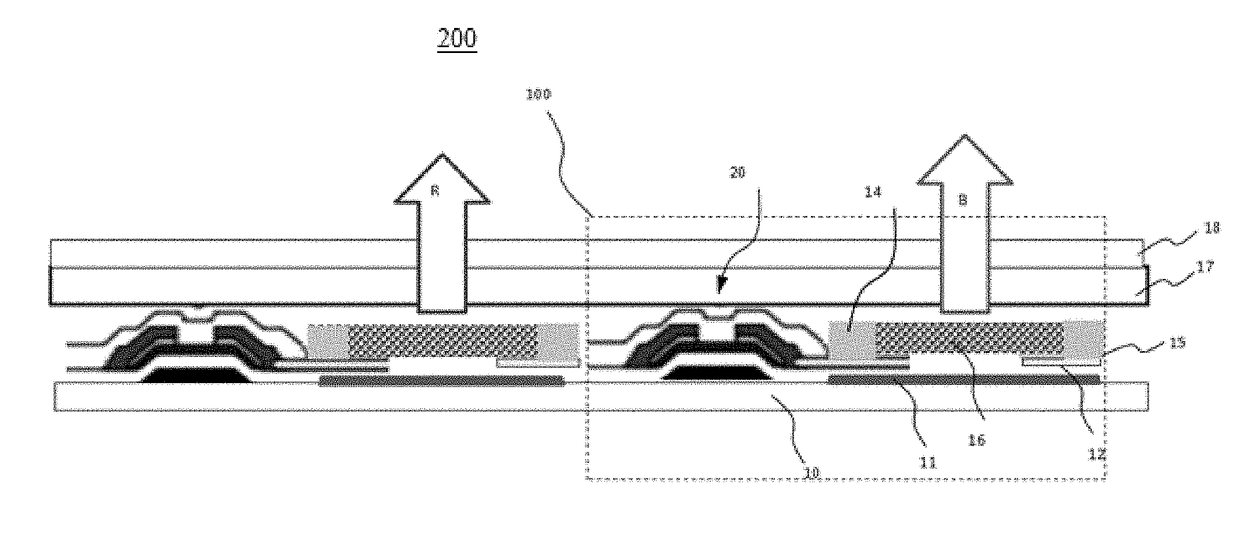
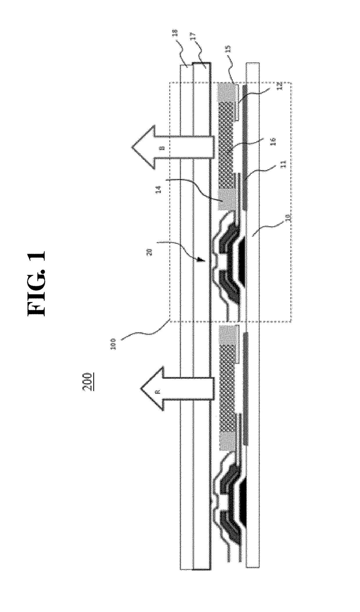
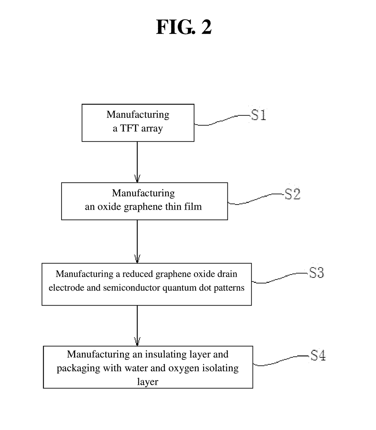
[0015]The present disclosure provides a method of manufacturing a graphene light emitting display, a characteristic that the degrees of reduction of graphene oxide are different at different light irradiating time is used, so that a source electrode, a drain electrode and a graphene quantum dot layer of a light emitting device can be manufactured by using one photomask.

[0016]As shown in FIG. 1, a graphene light emitting display 200 of th...


PUM

PropertyMeasurementUnit
operational wavelengthaaaaaaaaaa
operating voltageaaaaaaaaaa
voltageaaaaaaaaaa

Abstract

A graphene light emitting display and a method of manufacturing the same are disclosed. The method comprises: manufacturing a graphene oxide (GO) thin film on a surface of a substrate with a thin film transistor formed thereon; providing a photomask corresponding to the GO thin film to form a source electrode, a drain electrode and a graphene quantum dot layer of a graphene light emitting transistor; and wherein the photomask includes: a complete transparent part corresponding to the region in which the source electrode and the drain electrode are located; a light blocking part corresponding to the region in which the thin film transistor is located; and a semitransparent part corresponding to the region in which the graphene quantum dot layer is located; wherein an insulating layer and a water and oxygen isolating layer are formed sequentially on a surface of the substrate with the graphene light emitting transistor formed thereon.

Description

TECHNICAL FIELD[0001]The present disclosure belongs to a technical field of a liquid crystal display, and particularly, relates to a novel graphene light emitting display and a method of manufacturing the same.BACKGROUND ART[0002]With the development of technology and the improvement of life requirements of people, graphene has excellent characteristics such as hard texture, high transparency (transmissivity≈97.7%), high thermal conductivity (up to 5300 W / m·K), a high electron mobility (more than 15000 cm2 / V·s) and so on, and its application on the display is gradually increasing in recent years, especially on a touch screen (as an alternative to a traditional transparent conductive thin film ITO) and in the aspect of LED.[0003]In recent years, due to the appearance of a graphene light emitting element, the application of the graphene in the field of display can be extended. The color of the light emitted by a graphene light emitting transistor manufactured by using a graphene mater...

Claims


Application Information

Patent Timeline
Patent Type & Authority Applications(United States)
IPC IPC(8): H01L33/00H01L27/15H01L33/06H01L33/34H01L33/40H01L33/44
CPCH01L33/0041H01L27/156H01L33/0054H01L33/06H01L33/34H01L33/405H01L33/44H01L2933/0016H01L21/84H01L33/36H10K59/1213H10K85/20H10K50/844H10K59/1201
Inventor FAN, YONG
Owner SHENZHEN CHINA STAR OPTOELECTRONICS TECH CO LTD
Why Eureka
Try Eureka