

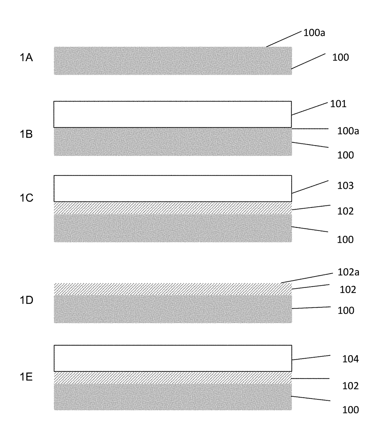
Process for indium or indium alloy deposition and article
a technology of indium or indium alloy and deposition process, which is applied in the direction of superimposed coating process, liquid/solution decomposition chemical coating, coating, etc., can solve the problems of high undesired use of cyanide, inability to use alkaline media in the later stages of printed circuit manufacturing and semiconductors, and inability to achieve the effect of submicron regim
- Summary
- Abstract
- Description
- Claims
- Application Information
AI Technical Summary
Benefits of technology
Problems solved by technology
Method used
Image

Examples
example 2 (
Inventive)
[0142]A substrate having a nickel surface (the sample) was immersed into the indium or indium alloy plating bath of Example 1 at 20° C. to deposit indium thereon. The potential for the indium deposition was −1.1 V (step ii.). After 15 seconds the potential was changed to −0.3 V to strip indium from the composed phase layer (step iii.). As soon as the current became constant which indicated that substantially all of the indium not formed into the composed phase layer was removed, the potential was changed to −1.1 V again. The deposition was continued until a total electrical charge of 0.55 C / cm2 was applied (step iv.). The sample was then removed from the indium or indium alloy plating bath, rinsed and dried.
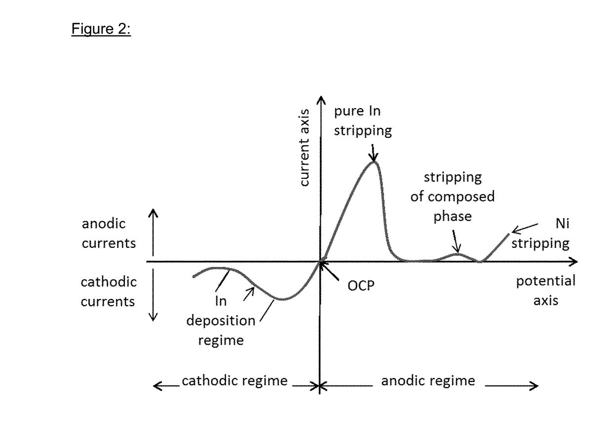
[0143]From the current-voltage-curve depicted in FIG. 3, useful working potentials for the deposition and stripping of indium can be obtained. After this indium deposition, the sample was analysed. From a visual inspection, the surface was much more even and much less d...
example 4 (
Inventive)
[0146]The process outlined in Example 2 was repeated and indium was deposited on a substrate having a ruthenium surface. A current-voltage-curve was used to identify a useful working potential for the deposition of indium which was determined to be −1.4 V in this case. Otherwise, the same parameters and the same aqueous indium or indium alloy plating bath as given in Example 2 were used. The surface of the sample had an average roughness of Sa=49.1 nm and the relative surface area increase (RSAI) was 3.1%.
[0147]The average roughness obtained in this inventive Example was around 35% smaller than the value obtained from the respective comparative Example 3.
example 6 (
Inventive)
[0149]The process outlined in Example 2 was repeated and indium was deposited on a substrate having a CoWP (cobalt tungsten phosphorous alloy) surface. A current-voltage-curve was used to identify a useful working potential for the deposition of indium which was determined to be −1.2 V in this case. Otherwise, the same parameters and the same aqueous indium or indium alloy plating bath as given in Example 2 were used. The surface of the sample had an average roughness of Sa=61 nm.
[0150]The average roughness obtained in this inventive Example was around 24% smaller than the value obtained from the respective comparative Example 5.
PUM
| Property | Measurement | Unit |
|---|---|---|
| Thickness | aaaaa | aaaaa |
| Nanoscale particle size | aaaaa | aaaaa |
| Thickness | aaaaa | aaaaa |
Abstract
Description
Claims
Application Information