
Pixel structure of OLED display panel and manufacturing method thereof

Active Publication Date: 2018-11-01
SHENZHEN CHINA STAR OPTOELECTRONICS SEMICON DISPLAY TECH CO LTD
View PDF2 Cites 3 Cited by
  • Summary
  • Abstract
  • Description
  • Claims
  • Application Information

AI Technical Summary

Benefits of technology

The present patent aims to improve the pixel structure by increasing the areas of sub-pixels formed in the sub-pixel region group. This facilitates the formation of sub-pixels and improves their thickness uniformity, reducing the possibility of generating mura and improving the utilization of pixel materials. The patent provides a manufacturing method for this pixel structure.

Problems solved by technology

Since a space in each slot of each sub-pixel region is small, the nozzle is not easily aligned with the sub-pixel regions.
In addition, since the space in each slot of each sub-pixel region is small, the pixel material in the slots easily overflow when a few drops of pixel material are dropped from the nozzle.

Method used


Image

  • Pixel structure of OLED display panel and manufacturing method thereof
  • Pixel structure of OLED display panel and manufacturing method thereof
  • Pixel structure of OLED display panel and manufacturing method thereof

Examples


first embodiment

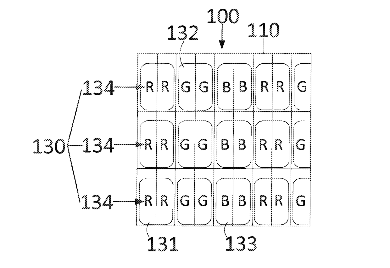
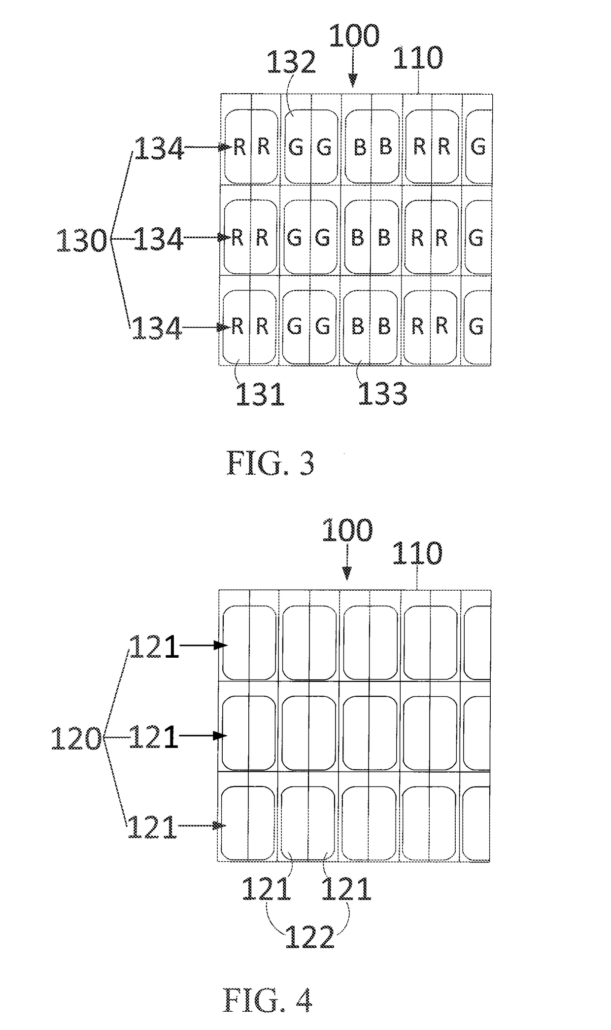
[0079]The first embodiment of the present configurations is shown in FIGS. 3 to 5. FIG. 3 is a structural diagram that illustrates a pixel structure in accordance with the first embodiment of the present configurations. FIG. 4 is a structural diagram that illustrates a pixel region in accordance with the first embodiment of the present configurations. FIG. 5 is a diagram of a cross-section structure illustration of a pixel structure in accordance with the first embodiment of the present configurations. The embodiment of the present configurations will be described in detail with reference to the pixel structure of the OLED display panel. It should be noted that the description of the pixel structure is also applicable to the OLED display panel or the OILED display.

[0080]The pixel structure 100 in the first embodiment of the present configurations comprises a substrate 110, a pixel region 120, a plurality of pixel units 130, at least two anode conductive layers 140, and a cathode con...

second embodiment

[0099]The second embodiment of the present configurations is shown in FIGS. 6 to 7. FIG. 6 is a structural diagram that illustrates a pixel structure in accordance with the second embodiment of the present configurations. FIG. 7 is a structural diagram that illustrates a pixel region in accordance with the second embodiment of the present configurations. FIGS. 6 to 7 are cooperated with FIGS. 3 to 5. The embodiment of the present configurations will be described in detail with reference to the pixel structure of the OLED display panel. It should be noted that the description of the pixel structure is also applicable to the OLED display panel or the OLED display.

[0100]The pixel structure 200 in the second embodiment of the present configurations comprises a substrate 210, a pixel region 220, a plurality of pixel units 230, a plurality of anode conductive layers, and a cathode conductive layer.

[0101]The substrate 210 may be referred to the substrate 110 in the first embodiment.

[0102]R...

third embodiment

[0109]The third embodiment of the present configurations is shown in FIG. 8. FIG. 8 is a diagram of a flowchart of a manufacturing method of a pixel structure in accordance with a third embodiment of the present configurations. FIG. 8 is cooperated with FIGS. 3 to 7. The manufacturing method of the pixel structure comprises steps of:

[0110]Step S101, forming at least two anode conductive layers on a substrate.

[0111]Step S102, forming a pixel region on the substrate, the pixel region comprising a plurality of sub-pixel regions arranged in sequence, at least two adjacent sub-pixel regions defined as a sub-pixel region group, at least two sub-pixel regions disposed integrally in the sub-pixel region group; forming two of the at least two anode conductive layers in the sub-pixel region respectively, the anode conductive layers in the sub-pixel region group separated from each other.

[0112]Step S103, forming a plurality of pixel units in the pixel region, each of the pixel units comprising...


PUM


Abstract

A pixel structure of an organic light emitting diode (OLED) display panel and a manufacturing method thereof are disclosed. The pixel structure comprises a pixel region, anode conductive layers, pixel units, and a cathode conductive layer. The pixel region comprises sub-pixel regions arranged in sequence, at least two adjacent sub-pixel regions defined as a sub-pixel region group are disposed integrally. The anode conductive layers are disposed in the sub-pixel regions respectively, and separated from each other. The cathode conductive layer is electrically connected with the anode conductive layers to control the pixel units. Each of the pixel units comprises sub-pixels and is disposed in the pixel region. Each of the sub-pixels is disposed in one of the sub-pixel regions. The sub-pixels are formed integrally and have a same color in the sub-pixel region group. The pixel unit comprises a hole injection layer, a luminous layer and an electron injection layer.

Description

FIELD OF THE INVENTION[0001]The present disclosure relates to the technical field of display manufacturing, and particularly to a pixel structure of an organic light emitting diode (OLED) display panel and a manufacturing method thereof.BACKGROUND OF THE INVENTION[0002]Known display types mainly include liquid crystal displays and organic light emitting diode (OLED) displays. Liquid crystal displays have advantages such as having a thin body, reduced power consumption, low radiation, etc, as well as being widely used. Most of the liquid crystal displays on the market are backlight type liquid crystal displays. Each backlight type liquid crystal display includes a liquid crystal panel and a backlight module. Working principle of the liquid crystal panel disposes liquid crystal molecules between two parallel glass substrates, applying a driving voltage between the glass substrates to control rotational direction of the liquid crystal molecules, and then generating a picture by light t...

Claims


Application Information

Patent Timeline
IPC IPC(8): H01L27/32H01L51/56
CPCH01L27/3218H01L27/3246H01L51/56H10K59/353H10K50/171H10K59/8052H10K71/00H10K59/8051H10K71/135H10K50/17H10K50/80H10K59/00H10K59/122
Inventor IGUCHI, SHINSUKEWU, YUAN-CHUNCAI, YUYING
Owner SHENZHEN CHINA STAR OPTOELECTRONICS SEMICON DISPLAY TECH CO LTD
Features
  • Generate Ideas
  • Intellectual Property
  • Life Sciences
  • Materials
  • Tech Scout
  • Unparalleled Data Quality
  • Higher Quality Content
  • 60% Fewer Hallucinations
Learn More