Grounded capacitance multipliers with electronic tuning possibility using single current feedback amplifier

a technology of capacitance multiplier and feedback amplifier, which is applied in the direction of impedence network, network simulating reactance, electrical apparatus, etc., can solve the problems of excessive capacitance value, unfeasible manufacturing cost of physically large capacitors, and high cost of realizing large capacitors on integrated circuits

Active Publication Date: 2018-12-06
YEDITEPE UNIVSI
View PDF0 Cites 1 Cited by
  • Summary
  • Abstract
  • Description
  • Claims
  • Application Information

AI Technical Summary

Benefits of technology

[0031]The main objective of the present patent application disclosed herein is to realize a C-multiplier circuit which is suitable for monolithic integration using CMOS...

Problems solved by technology

In a conventional fabrication process, realization of a physically large capacitor on an integrated circuit is very costly unless special fabrication process steps have been added to implement it.
Real physical capacitors with capacitance values higher than 100 pF are considered to be a physically large capacitor with unfeasible manufacturing costs.
One solution of this problem is to employ a Capacitance Multiplier circuit in place of a real physical capacitor with excessively large capacitance value.
The frequency response stability of the overall circuit may be adversely affected.
One apparent disadvantage of the circuit described by U.S. Pat. No. 3,911,296 is that the resultant capacitance is a function of the beta of the transistor which itself is process and temperature dependent.
Another disadvantage of the circuit of U.S. Pat. No. 3,911,296 is that on-chip capacitor takes up die area of the integrated circuit chip.
This circuit 1 has the advantage of using single active element (Op-amp) but has a disadvantage of being far from pure capacitance simulator.
Therefore, this circuit can only simulate a lossy capacitance.
On the other hand, lossy C-multipliers involve many unwanted parasitic terms and noise sources which increase by thermal agitation.
These become strongly dis...

Method used


Image

  • Grounded capacitance multipliers with electronic tuning possibility using single current feedback amplifier
  • Grounded capacitance multipliers with electronic tuning possibility using single current feedback amplifier

Examples


Embodiment Construction

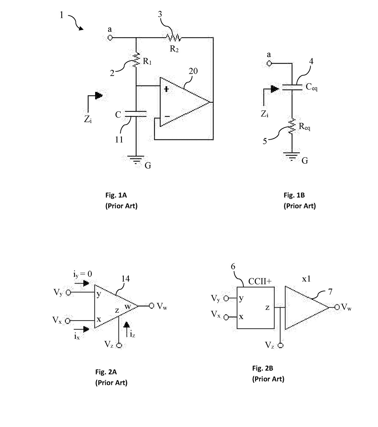
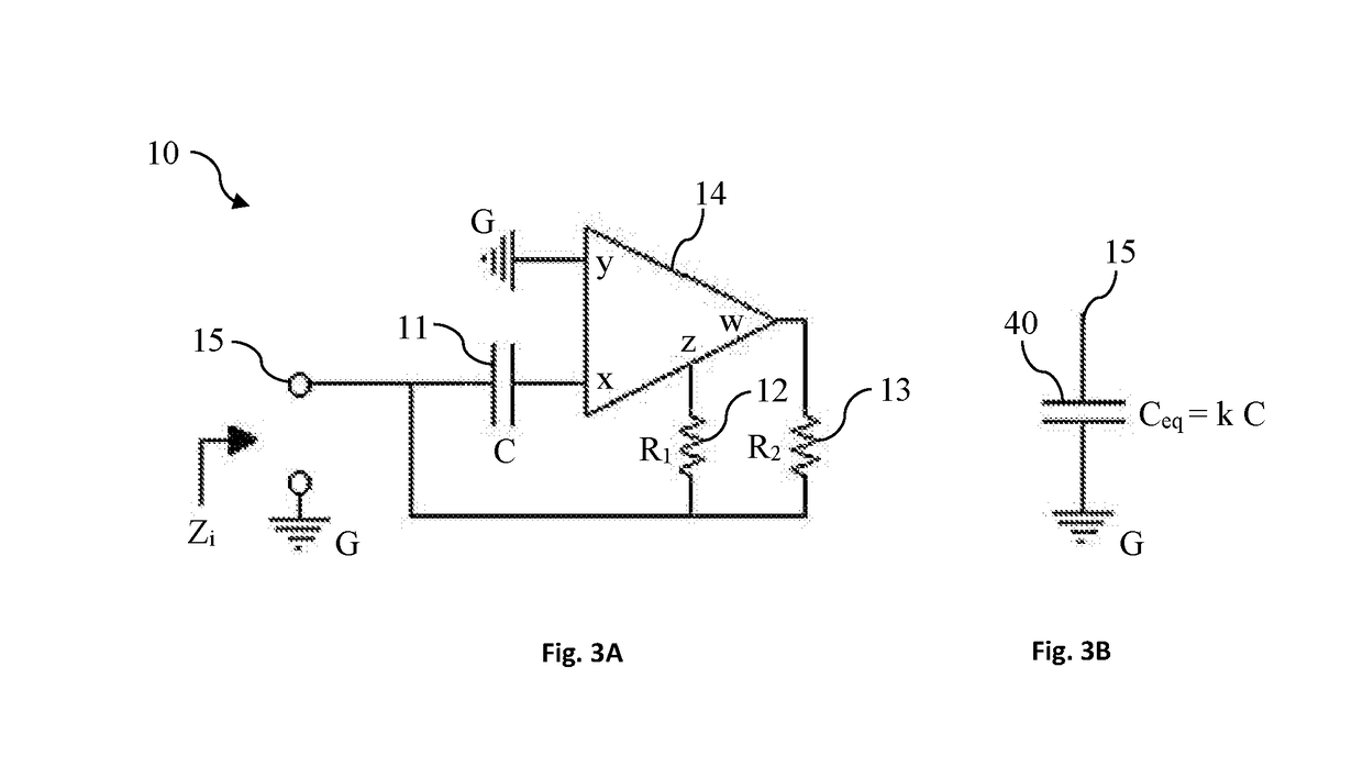
[0049]First preferred embodiment of the present invention is displayed in FIG. 3A. The capacitance multiplier circuit comprises; a current feedback operational amplifier (CFOA) 14 having x, y, z and w-terminal and in which a plus type current conveyor (CCII+) is employed; a capacitor 11 having a first end connected to the x-terminal of the CFOA 14 and a second end connected to an input node 15; a first resistor 12 having a first end connected to the z-terminal of the CFOA 14 and a second end connected to the second end of the capacitor 11; a second resistor 13 having a first end connected to the w-terminal of the CFOA 14 and a second end connected to the second end of the first resistor 12.

[0050]In this embodiment, either the first resistor 12 or the second resistor 13 or both of said resistors can be constructed as different types of resistor such as voltage or current controlled resistor.

[0051]Here, equivalent input impedance of the Capacitance Multiplier circuit 10 is a pure (los...


PUM


Abstract

The present invention relates to a capacitance multiplier topology suitable for both positive and negative capacitance multiplication having a minimum configuration consisting of a current feedback amplifier (CFOA), two resistors and a reference capacitor, with each C-multiplier having a respective capacitance amplification constant k which is externally adjustable. Such a capacitance multiplier has less parasitic components, occupies a smaller chip area with higher simulated capacitance value.

Description

FIELD OF THE INVENTION[0001]Present invention relates generally to integrated Capacitance Multiplier circuits, and particularly to grounded Capacitance Multiplier circuits (Capacitance Amplifiers) of positive and negative simulated capacitance values using a single Current Feedback Amplifier.BACKGROUND OF THE INVENTION[0002]Capacitor is an electronic component that stores electric charge. In a conventional fabrication process, realization of a physically large capacitor on an integrated circuit is very costly unless special fabrication process steps have been added to implement it. Real physical capacitors with capacitance values higher than 100 pF are considered to be a physically large capacitor with unfeasible manufacturing costs. Therefore, such a physically large capacitor construction should be avoided. One solution of this problem is to employ a Capacitance Multiplier circuit in place of a real physical capacitor with excessively large capacitance value.[0003]Capacitance mult...

Claims


Application Information

Patent Timeline
IPC IPC(8): H03H11/48
CPCH03H11/483H03H2011/0477H03H2210/028
Inventor KESKIN, ALI UMIT
Owner YEDITEPE UNIVSI
Why Eureka
Try Eureka