Reduction of wafer bow during growth of epitaxial films

Inactive Publication Date: 2018-12-13
MACOM TECH SOLUTIONS HLDG INC
View PDF3 Cites 4 Cited by
  • Summary
  • Abstract
  • Description
  • Claims
  • Application Information

AI Technical Summary

Benefits of technology

[0005]Structures and methods for reducing wafer bow in heteroepitaxy are described. In some embodiments, micro-trenches are formed across a surface of a substrate that is used for heteroepitaxial overgrowth. The trenches are filled with a material before overgrowth. Non-mon

Problems solved by technology

Although GaN is a desirable semiconductor material for many applications, it is more expensive to produce than conventional silicon semiconductor wafers.
However, due to mismatches in material properties, such heteroepitaxy can lead to in-plane stresses in the GaN layer and cause out-of-plane wa

Method used


Image

  • Reduction of wafer bow during growth of epitaxial films
  • Reduction of wafer bow during growth of epitaxial films
  • Reduction of wafer bow during growth of epitaxial films

Examples


Embodiment Construction

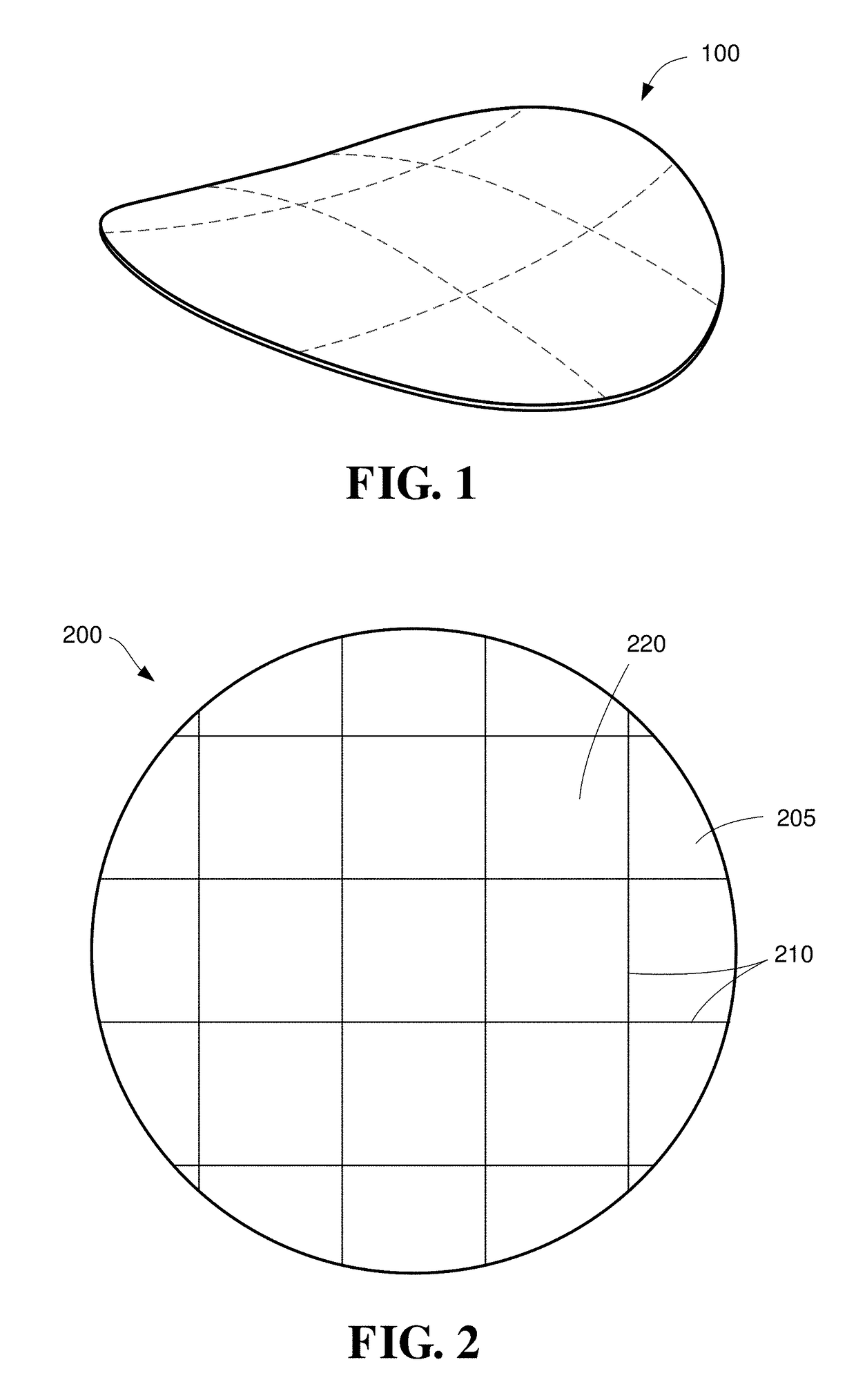
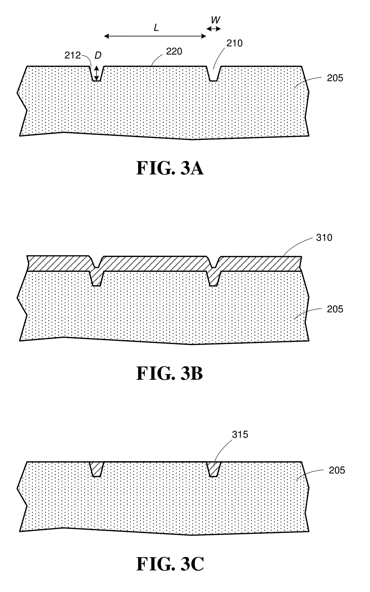
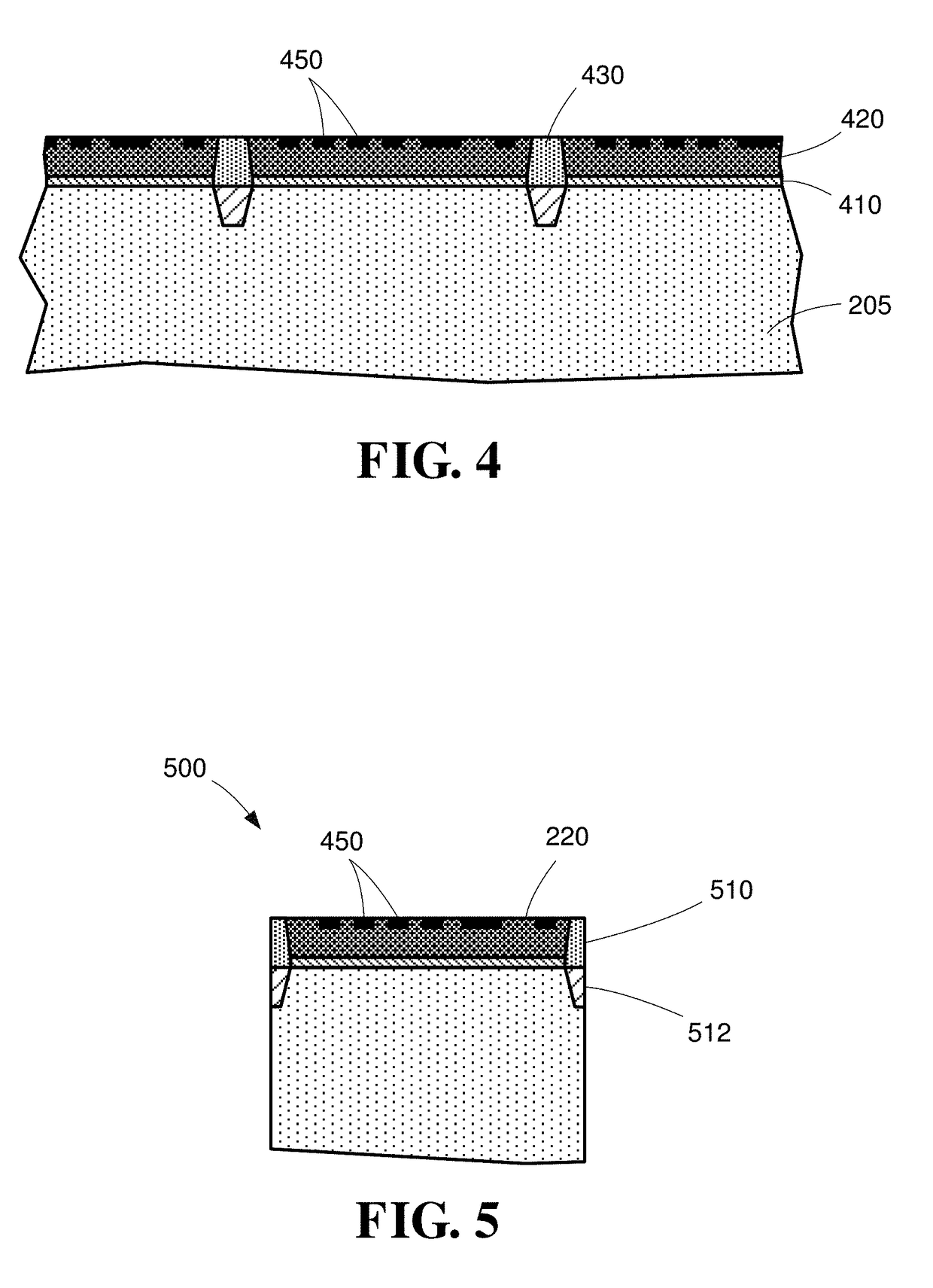
[0025]Heteroepitaxy has become a useful process for forming high-performance or specialized semiconductor materials at reduced cost and large wafer sizes compared to forming bulk substrates of a desired semiconductor material. In heteroepitaxy, a desired monocrystalline semiconductor material is grown over a dissimilar crystalline material. The heteroepitaxy layer may be formed using a chemical vapor deposition process, for example, or any other suitable crystal-growth process. Some examples of heteroepitaxial systems include gallium-nitride materials grown on silicon, silicon-carbide, or sapphire substrates. There are many other heteroepitaxy systems, and the technology described herein is not limited to only gallium-nitride materials. Examples of other heteroepitaxy systems include, but are not limited to, any of silicon-carbide, silicon-germanium, gallium-arsenide materials, gallium-phosphide materials, and indium-phosphide materials grown on silicon or other substrate materials....


PUM


Abstract

Structures and methods for reducing wafer bow during heteroepitaxial growth are described. Micro-trenches may be formed across a surface of a substrate and filled with polycrystalline material. Stress-relieving regions of material can be grown over the polycrystalline material in a layer of semiconductor material during heteroepitaxy.

Description

BACKGROUNDTechnical Field[0001]The technology relates to epitaxial growth of crystalline layers on semiconductor wafers.Discussion of the Related Art[0002]Gallium-nitride semiconductor material has received appreciable attention in recent years because of its desirable electronic and electro-optical properties. Gallium nitride (GaN) has a wide, direct bandgap of about 3.4 eV that corresponds to the blue wavelength region of the visible spectrum. Light-emitting diodes (LEDs) and laser diodes (LDs) based on GaN and its alloys have been developed and are commercially available. These devices can emit visible light ranging from the violet to red regions of the visible spectrum.[0003]Because of its wide bandgap, gallium nitride is more resistant to avalanche breakdown and has a higher intrinsic field strength compared to more common semiconductor materials, such as silicon and gallium arsenide. In addition, gallium nitride is a wide bandgap semiconductor and is able to maintain its elect...

Claims


Application Information

Patent Timeline
IPC IPC(8): H01L21/02H01L29/20H01L33/00H01L33/32C30B29/40C30B25/18H01S5/24H01S5/02H01S5/323
CPCH01L21/0243H01S2301/173H01L21/02378H01L21/0242H01L21/02499H01L21/0254H01L29/2003H01L33/007H01L33/32C30B29/406C30B25/183H01S5/24H01S5/0206H01S5/32341H01S5/0205H01L21/02381H01L21/02592H01L21/02595H01L21/02598
Inventor CARLSON, DOUGLASBOLES, TIMOTHY E.
Owner MACOM TECH SOLUTIONS HLDG INC
Why Eureka
Try Eureka