Waveguide-to-microstrip transition

a waveguide and microstrip technology, applied in the field of microwave frequency devices, can solve the problems of poor performance, high manufacturing cost, and high complexity, and achieve the effect of low insertion loss and wide bandwidth

Active Publication Date: 2018-12-13
OBSHCHESTVO S OGRANICHENNOJ OTVETSTVENNOSTYU RADIO GIGABIT
View PDF0 Cites 8 Cited by
  • Summary
  • Abstract
  • Description
  • Claims
  • Application Information

AI Technical Summary

Benefits of technology

[0013]The object of the present invention is to provide a probe-type waveguide-to-microstrip transition with wide bandwidth and low insertion loss, the transition comprising a structure which does not produce parasitic capacitance of the impedance between the probe and the waveguide channel.

Problems solved by technology

Drawbacks of such transition include high complexity and therefore high manufacturing cost.
Furthermore, there are some issues related to the positioning of the board in the waveguide channel leading to worse performance and poor repeatability.
These disadvantages are further amplified with the increase of operational frequencies to the millimeter-wave range.
Moreover, such transition requires several dielectric layers on the board, thus increasing structure complexity and sensitivity of the transition to manufacturing error.
Finally, the presence of the dielectric board inside the waveguide channel leads to additional signal loss related to dielectric loss in the substrate.
Owing to such an arrangement, the transition experiences high level of parasitic radiation from the board end face that leads to significant insertion loss.
Moreover, the need for manufacturing two metal parts forming a waveguide channel leads to strict requirements for flatness and surface roughness which lead to an increase in manufacturing costs.
The main drawback of the prior-art transition is the emergence of an equivalent LC circuit (resonant circuit) formed by the waveguides and a portion of the dielectric board that is located inside the waveguide channel.
These elements significantly complicate the transition design and decrease manufacturing tolerances.
Another disadvantage is an increase in insertion loss between the line and the waveguide which is caused by the presence of the dielectric board substrate in the waveguide channel area.

Method used


Image

  • Waveguide-to-microstrip transition
  • Waveguide-to-microstrip transition

Examples


Embodiment Construction

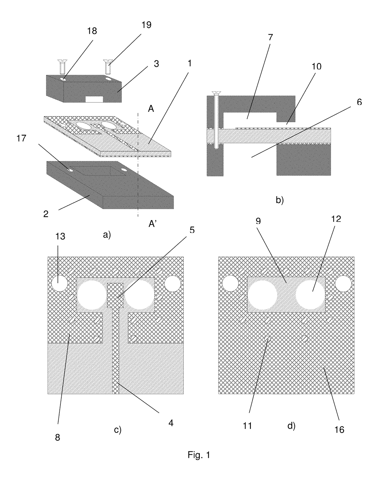
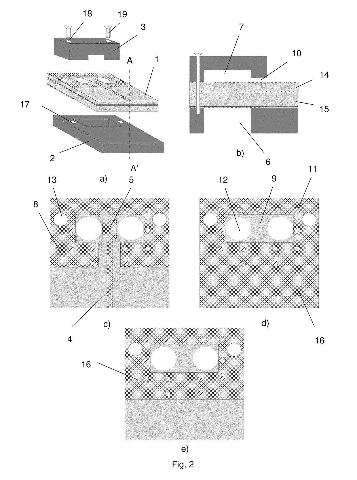
[0063]A waveguide-to-microstrip transition comprises an input waveguide piece 2 having a through-hole defining an open waveguide channel 6, a short-circuited waveguide piece 3 having a blind cavity defining a closed waveguide channel 7, and a dielectric board 1 placed between the waveguides pieces 2, 3. The top surface of the dielectric board 1 comprises a microstrip transmission line 4, a microstrip probe 5 formed as an extension of the microstrip transmission line 4, and a contact metal layer 8 surrounding the microstrip probe 5 with no electrical connection to the microstrip probe 5 and the microstrip transmission line 4, wherein the contact metal layer 8 forms an internal area on the dielectric board 1, the internal area being a waveguide channel area 9.

[0064]The waveguide short-circuited piece 3 is located on the contact metal layer 8 and has a recess 10 in the area of the microstrip transmission line 4, while the bottom surface of the dielectric board 1 comprises a ground meta...


PUM


Abstract

The invention relates to microwave technology and can be used in measuring technology and wireless communication. The technical result is a waveguide-to-microstrip transition which provides reduced signal transmission losses and increased working bandwidth together with a low wave reflection coefficient. A contacting metal layer is arranged on an upper surface of a dielectric circuit board around a micro-strip probe, without electrical contact with the micro-strip probe and a micro-strip transmission line and forming an internal area on the dielectric circuit boar being a waveguide channel area. A closed waveguide section having a slot in the area of the microstrip transmission line is arranged on the contacting metal layer. At least one metallized transition through-hole is formed along a perimeter around the area of the waveguide channel in the metal layers and in the dielectric circuit board, and at least one non-metallized through-hole is formed inside the waveguide channel area.

Description

FIELD OF THE INVENTION[0001]The present invention generally relates to the field of microwave frequency devices and more specifically to waveguide-to-microstrip transitions which provide effective transfer of electromagnetic energy between a metal waveguide and a microstrip line realized on a dielectric board. The invention can be used in measurement equipment, antenna systems and in various wireless communication systems and radars.BACKGROUND OF THE INVENTION[0002]One of the trends in modern wireless communication systems is frequency band extension with simultaneous carrier frequency shift to the millimeter-wave range. In the millimeter-wave region (30-300 GHz) of electromagnetic spectrum, such applications as indoor local radio networks, radio relay links, automotive radars, microwave imaging devices etc. are already successfully used. For example, communication systems operating in the millimeter-wave range provide significant improvement in data transmission throughput of up to...

Claims


Application Information

Patent Timeline
Patent Type & Authority Applications(United States)
IPC IPC(8): H01P5/107H01P1/04H01Q1/50H01Q13/10
CPCH01P5/107H01P1/042H01Q1/50H01Q13/106
Inventor ARTEMENKO, ALEKSEY ANDREEVICHMASLENNIKOV, ROMAN OLEGOVICHMOZHAROVSKIY, ANDREY VIKTOROVICHSOYKIN, OLEG VALER'EVICHSSORIN, VLADIMIR NIKOLAEVICH
Owner OBSHCHESTVO S OGRANICHENNOJ OTVETSTVENNOSTYU RADIO GIGABIT
Why Eureka
Try Eureka