Manufacturing method of flexible TFT substrate

Active Publication Date: 2018-12-20
WUHAN CHINA STAR OPTOELECTRONICS SEMICON DISPLAY TECH CO LTD
View PDF0 Cites 8 Cited by
  • Summary
  • Abstract
  • Description
  • Claims
  • Application Information

AI Technical Summary

Benefits of technology

[0032]Compared to the known techniques, the present invention provides the following advantages. The present invention provides a manufacturing method of flexible TFT substrate, wherein a first contact hole is formed above the two sides of the active layer and a buffer hole is formed on the flexible base substrate after depositing a silicon oxide layer of the interlayer dielectric layer, and then coating the organic photo-resist material on the silicon oxide layer and filling the organic photo-resist material into the buffer hole during the coating process to form an organic photo-resist layer to obtain an interlayer dielectric layer formed by the

Problems solved by technology

However, in recent years, flexible TFT technology is becoming more and more demanding, so the conventi

Method used


Image

  • Manufacturing method of flexible TFT substrate
  • Manufacturing method of flexible TFT substrate
  • Manufacturing method of flexible TFT substrate

Examples


Example

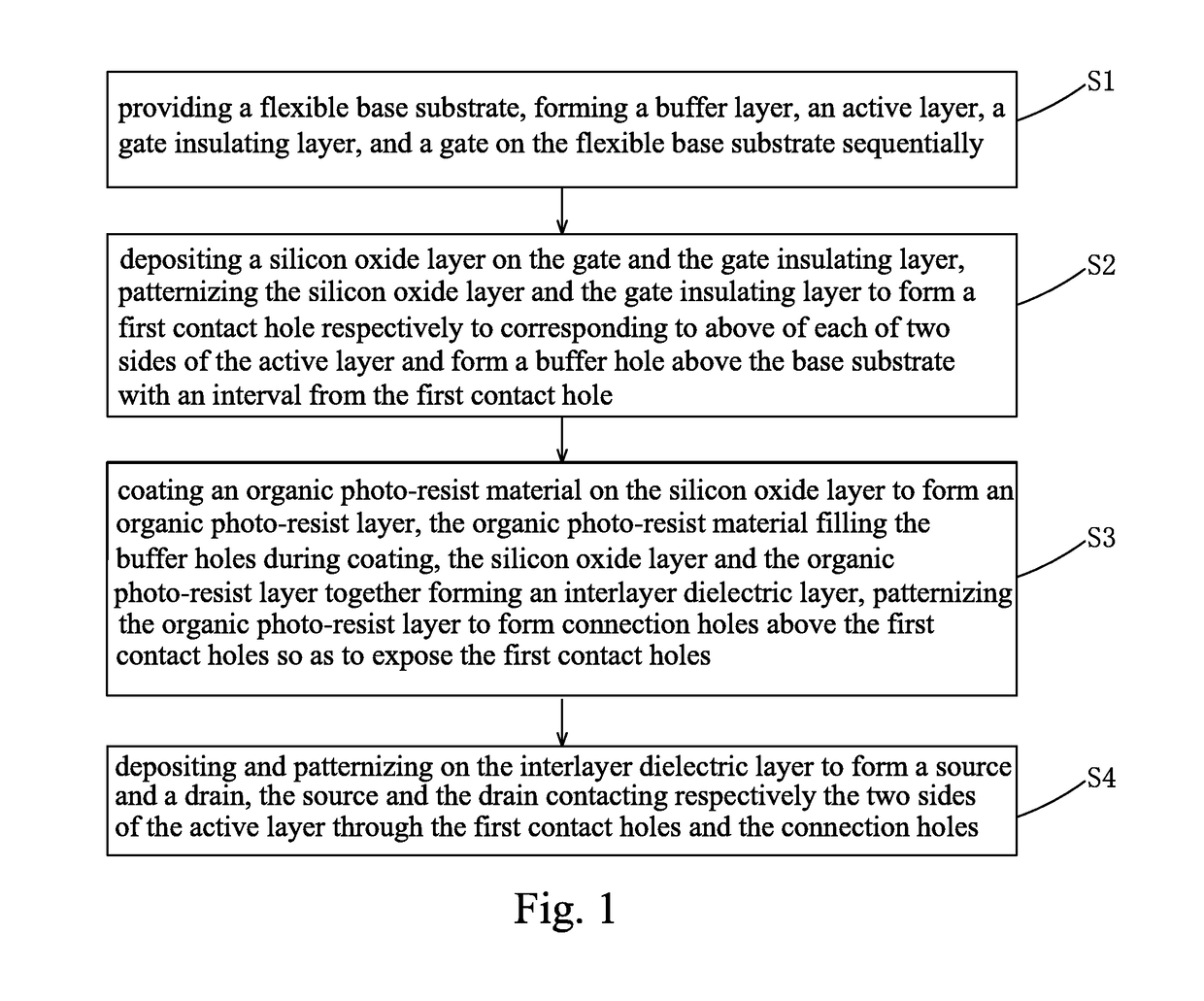
[0040]To further explain the technique means and effect of the present invention, the following uses preferred embodiments and drawings for detailed description.

[0041]Referring to FIG. 1, the present invention provides a manufacturing method of flexible TFT substrate, comprising the steps of:

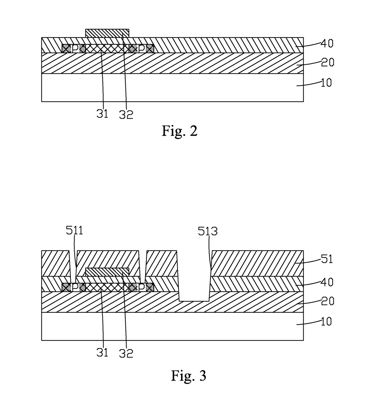
[0042]Step S1: as shown in FIG. 2, providing a flexible base substrate 10, depositing a buffer layer 20 on the flexible base substrate 10, depositing and patternizing to form an active layer 31 on the buffer layer 20, depositing a gate insulating layer 40 on the active layer 31 and the buffer layer 20, depositing and patternizing to form a gate 32 on the gate insulating layer 31.

[0043]Specifically, Step S1 of forming the active layer 31 comprises: depositing an amorphous silicon (a-Si) thin film on the buffer layer 20, converting the a-Si thin film into a polycrystalline silicon (poly-Si) thin film by an excimer laser annealing crystallization process, and then patternizing the polycrystalline s...


PUM


Abstract

The invention provides a manufacturing method of flexible TFT substrate, forming first contact hole above two sides of the active layer and buffer hole on flexible base substrate after depositing a silicon oxide layer of interlayer dielectric layer (ILD), coating organic photo-resist material on the silicon oxide layer and filling the organic photo-resist material into the buffer hole during coating to form organic photo-resist layer to obtain ILD including silicon oxide layer and organic photo-resist layer, and patternizing organic photo-resist layer to form a connection hole corresponding to above of first contact hole so that the subsequent source/drain connected to active layer through the first contact holes and connection holes. By replacing the silicon nitride layer in conventional ILD with flexible organic photo-resist layer and providing buffer hole filled with organic photo-resist material on flexible base substrate, the flexibility of TFT substrate is enhanced and product performance improved.

Description

BACKGROUND OF THE INVENTION1. Field of the Invention[0001]The present invention relates to the field of display techniques, and in particular to a manufacturing method of flexible TFT substrate.2. The Related Arts[0002]In the field of display technology, the panel display technology has replaced cathode ray tube (CRT) display. Because of the advantages of high display quality, low power-consumption, thinness and wide applications, the e panel display device has been widely used in mobile phones, TV, PDA, digital camera, notebook PC, desktop PC, and other consumer electronic products, and becomes the mainstream of the display device.[0003]The thin film transistor (TFT) is the main driving element used in the liquid crystal display (LCD) and active matrix organic light-emitting diode (AMOLED) display device, and is directly related to future progress of the high-performance panel display device.[0004]The TFT includes various structures, as well as various materials for manufacturing t...

Claims


Application Information

Patent Timeline
IPC IPC(8): H01L27/12H01L27/32H01L51/00H01L21/768
CPCH01L27/1288H01L27/3246H01L27/3262H01L51/0097H01L27/1218H01L27/127H01L27/1262H01L21/76802G02F2201/123H01L27/1248H10K77/111H10K59/122H10K59/1213
Inventor LI, SONGSHAN
Owner WUHAN CHINA STAR OPTOELECTRONICS SEMICON DISPLAY TECH CO LTD
Why Eureka
Try Eureka