

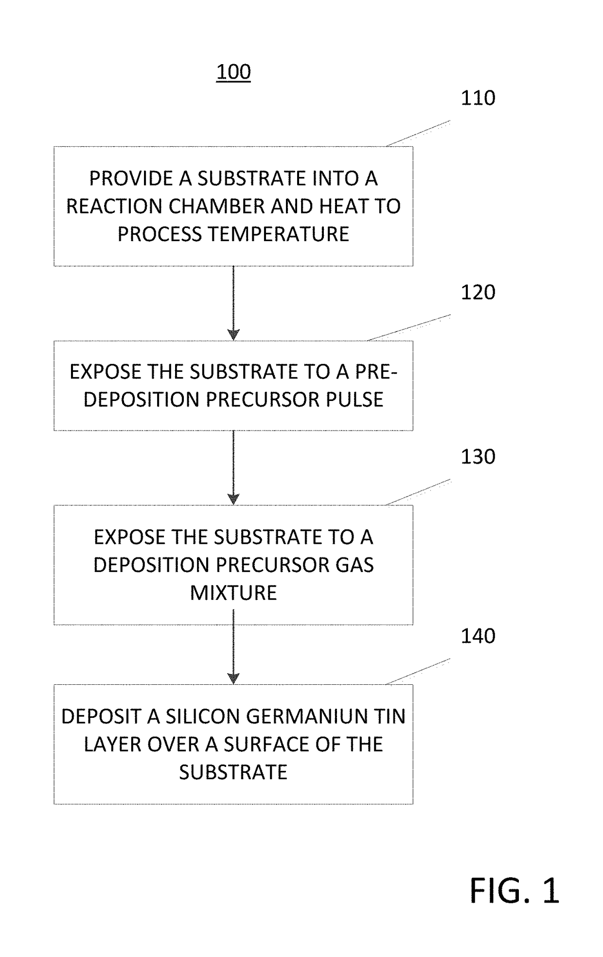
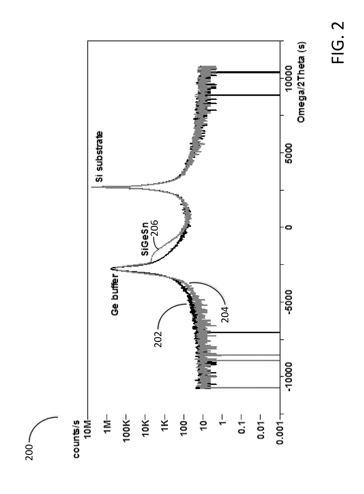
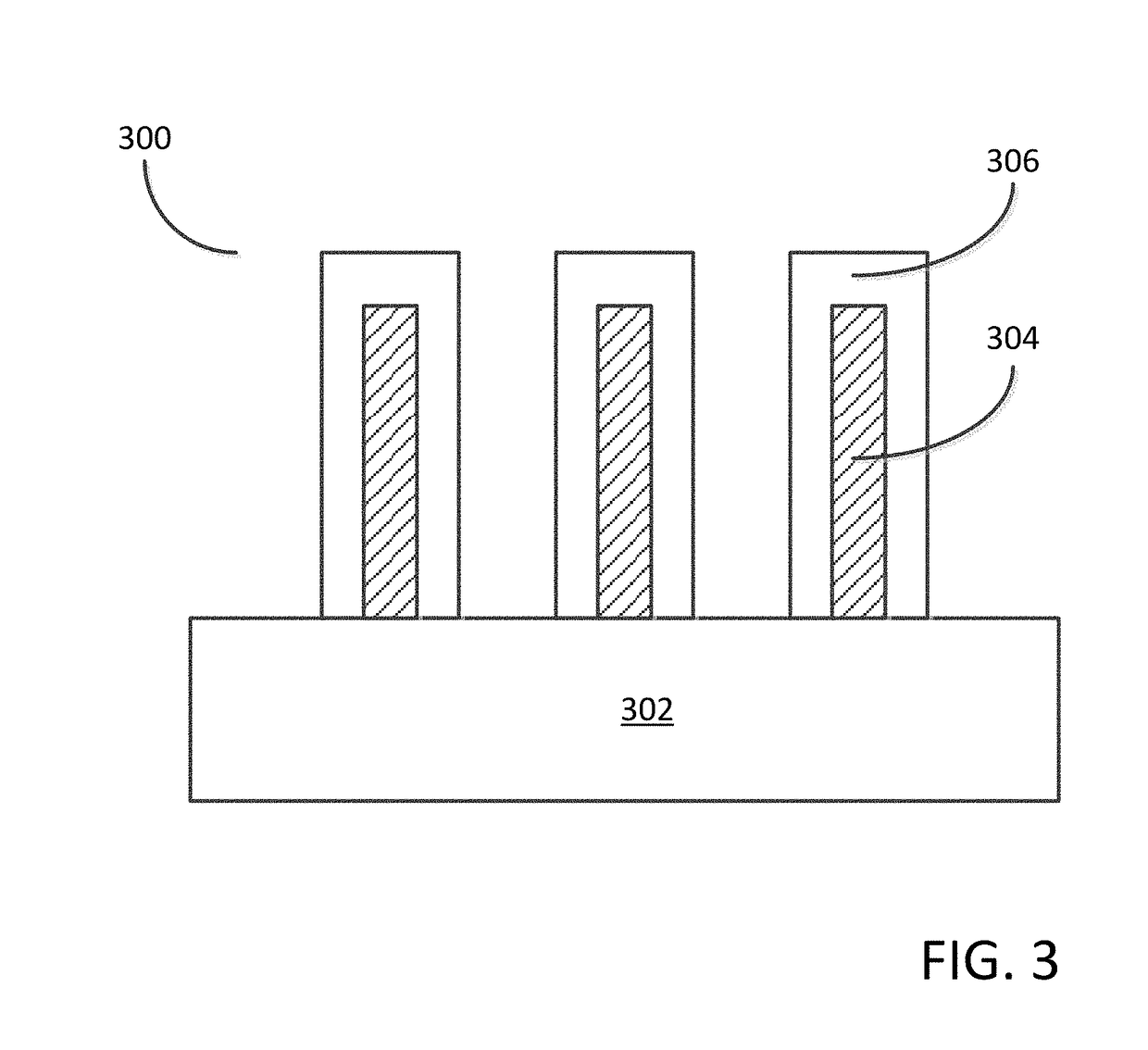
Methods for forming a silicon germanium tin layer and related semiconductor device structures
a technology semiconductor devices, which is applied in the direction of coatings, semiconductor devices, chemical vapor deposition coatings, etc., can solve the problems of silicon germanium tin (sigesn) on certain substrate surfaces and silicon germanium tin (sigesn) on the surface of a silicon substrate or a germanium substrate being extremely difficult to form
- Summary
- Abstract
- Description
- Claims
- Application Information
AI Technical Summary
Benefits of technology
Problems solved by technology
Method used
Image

Examples
Embodiment Construction
[0015]Although certain embodiments and examples are disclosed below, it will be understood by those in the art that the invention extends beyond the specifically disclosed embodiments and / or uses of the invention and obvious modifications and equivalents thereof. Thus, it is intended that the scope of the invention disclosed should not be limited by the particular disclosed embodiments described below.
[0016]As used herein, the term “substrate” may refer to any underlying material or materials that may be used, or upon which, a device, a circuit or a film may be formed.
[0017]As used herein, the term “epitaxial layer” may refer to a substantially single crystalline layer upon an underlying substantially single crystalline substrate.
[0018]As used herein, the term “hydrogenated silicon source” may refer to a source of silicon having hydrogen incorporated therein.
[0019]As used herein, the term “chemical vapor deposition” may refer to any process wherein a substrate is exposed to one or m...
PUM
| Property | Measurement | Unit |
|---|---|---|
| Temperature | aaaaa | aaaaa |
| Time | aaaaa | aaaaa |
| Thickness | aaaaa | aaaaa |
Abstract
Description
Claims
Application Information