Compound semiconductor device and method for manufacturing the same

Active Publication Date: 2019-01-31
DENSO CORP
View PDF3 Cites 4 Cited by
  • Summary
  • Abstract
  • Description
  • Claims
  • Application Information

AI Technical Summary

Benefits of technology

[0012]As described above, the introducing of the dopant gas including the second conductivity type dopant is started during the temperature increasing period and the introducing of the material gas is started during the temperature increasing period after the introducing the second conductivity type dopant gas. As such, the de

Problems solved by technology

When the corner portion of the bottom of the deep trench is changed to n-type, the p-type layer cannot sufficiently restrict the electrical field from breaking into the trench gate structure and the

Method used


Image

  • Compound semiconductor device and method for manufacturing the same
  • Compound semiconductor device and method for manufacturing the same
  • Compound semiconductor device and method for manufacturing the same

Examples


first embodiment

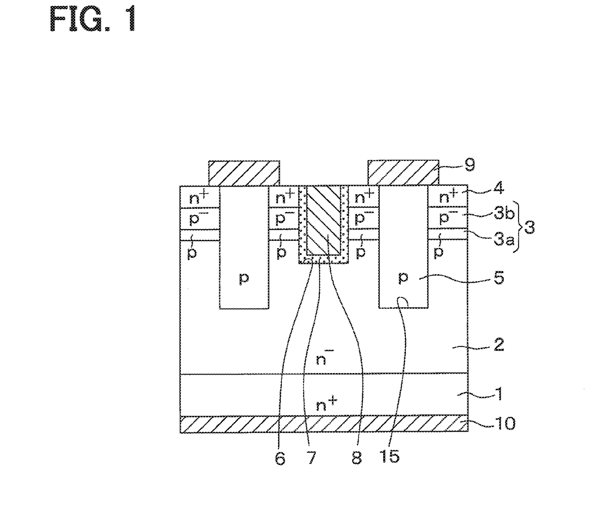
[0020]An SiC semiconductor device that includes a vertical MOSFET having an inverted type trench gate structure according to the present disclosure will be described with reference to FIG. 1.

[0021]An SiC semiconductor device illustrated in FIG. 1 includes a vertical MOSFET having a trench gate structure and disposed in a cell area. The SiC semiconductor device has an outer peripheral resistant structure, which is not shown, disposed in an outer peripheral area surrounding the cell area.

[0022]The SiC semiconductor device has a semiconductor substrate that includes an n+-type substrate 1 providing a high concentration impurity layer formed of SiC, and an n−-type drift layer 2 disposed on a front face side of the n+-type substrate 1 and formed of SiC having an impurity concentration lower than the impurity concentration of the n+-type substrate 1. For example, the n+-type substrate 1 has an n-type impurity concentration of 1.0×10¹⁹ / cm3, and a front face constituted by (0001) Si face. F...

second embodiment

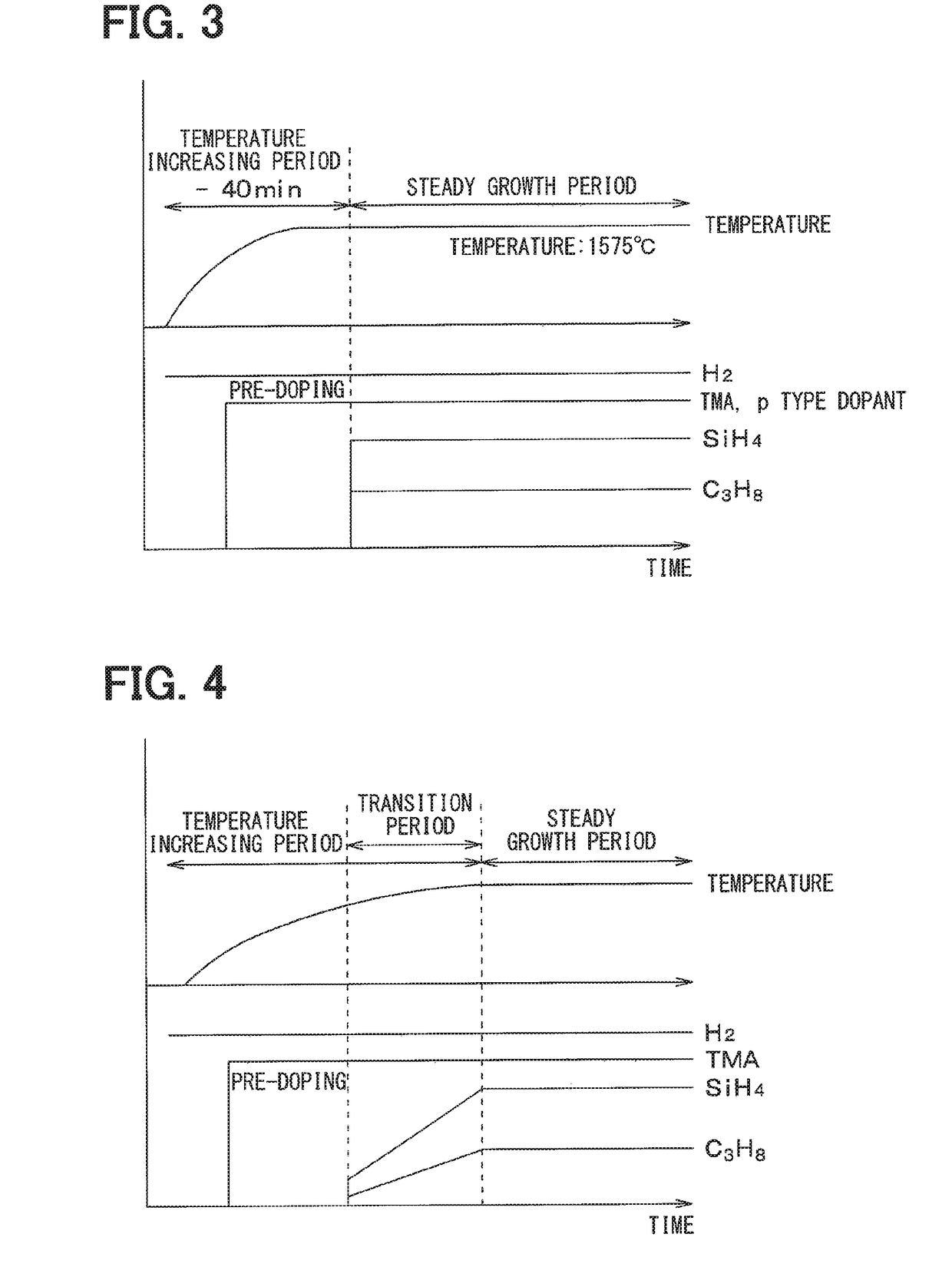
[0061]A second embodiment will be described. In the present embodiment, the introducing method of the SiC material gas is changed from the first embodiment. Since the other parts are similar to the first embodiment, only parts different from the first embodiment will be described.

[0062]As shown in FIG. 4, the introduction of the SiC material gas is started during the temperature increasing period. The introducing amount of the SiC material gas is decreased in the initial stage of the introducing and then gradually increased toward the desired introducing amount. The period in which the introducing amount of the SiC material gas is gradually increased is defined as a transition period and the period after the introducing amount of the SiC becomes constant is defined as a steady growth period. During the transition period, the epitaxial growth is conducted moderately. During the steady growth period, the epitaxial growth is conducted with desired growth rate, e.g., up to 4 μm / h. For e...

third embodiment

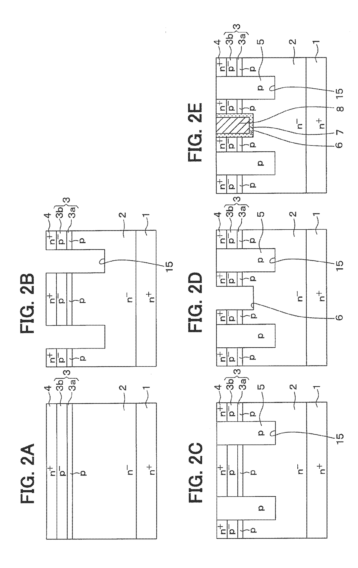
[0064]A third embodiment will be described. In the present embodiment, the structure of the p-type deep layer 5 and the introducing method of the SiC material gas are changed from the first embodiment and the second embodiment. Since the other parts are similar to the first embodiment and the second embodiment, parts different from the first embodiment and the second embodiment will be described. In the present embodiment, examples in which the introducing amount of the SiC material gas is changed similarly to the second embodiment. However, the introducing amount of the SiC may be constant similarly to the first embodiment.

[0065]As shown in FIG. 5, in the present embodiment, the bottom corner portion of the p-type deep layer 5, in other words, the bottom corner portion of the deep trench15 is provided by a p+-type region 5a. The p+-type region 5a is located below the base region 3 and separated from the base region 3. However, the p+-type region 5a may be connected to the base regi...


PUM


Abstract

A method for manufacturing a compound semiconductor device includes: providing a semiconductor substrate including a foundation layer having a first conductivity type; forming a deep trench in the foundation layer; and forming a deep layer having a second conductivity type by introducing material gas of the compound semiconductor while introducing dopant gas into an epitaxial growth equipment to cause epitaxial growth of the deep layer in the deep trench. A period in which a temperature in the epitaxial growth equipment is increased to a temperature of the epitaxial growth of the deep layer is defined as a temperature increasing period. In the forming the deep layer, the deep layer is further formed in a bottom corner portion of the deep trench by starting the introducing of the dopant gas during the temperature increasing period and starting the introducing of the material gas after the temperature increasing period.

Description

CROSS REFERENCE TO RELATED APPLICATION[0001]This application is based on Japanese Patent Application No. 2016-32293 filed on Feb. 23, 2016, the disclosure of which is incorporated herein by reference.TECHNICAL FIELD[0002]The present disclosure relates to a method for manufacturing a compound semiconductor device, and a compound semiconductor device, the device including a compound semiconductor such as silicon carbide (hereinafter referred to as SiC) and gallium nitride (hereinafter referred to as GaN).BACKGROUND ART[0003]Conventionally, patent literature 1 proposes an SiC semiconductor device including vertical metal-oxide-semiconductor field-effect transistor (MOSFET) having inverted type trench gate structure, as a vertical switching element having a trench gate structure. In the vertical MOSFET having the inverted type trench gate structure, a gate voltage is applied to a gate electrode in a gate trench, a channel is formed in a p-type base region located on a side surface of th...

Claims


Application Information

Patent Timeline
IPC IPC(8): H01L29/06H01L29/16H01L29/10H01L29/78H01L29/66H01L21/02H01L21/04
CPCH01L21/02579H01L21/0262H01L21/0475H01L21/049H01L21/02529H01L29/2003H01L29/1608H01L29/1095H01L29/7813H01L29/66068H01L29/063H01L21/02378H01L21/0243
Inventor TAKEUCHI, YUICHIAKIBA, ATSUYASUZUKI, KATSUMIYAMASHITA, YUSUKE
Owner DENSO CORP
Why Eureka
Try Eureka