Supercharge Your Innovation With Domain-Expert AI Agents!

Etching solution of igzo film layer and etching method of the same

a technology of etching solution and igzo film, which is applied in the direction of electrical equipment, chemistry apparatus and processes, and semiconductor devices, etc., can solve the problems of igzo vth (starting voltage) drift or leakage current, low mobility of as, and large impact, so as to effectively control the etching solution rate and raise the stability of igzo-tft devices

Inactive Publication Date: 2019-02-07
SHENZHEN CHINA STAR OPTOELECTRONICS SEMICON DISPLAY TECH CO LTD
View PDF4 Cites 2 Cited by
  • Summary
  • Abstract
  • Description
  • Claims
  • Application Information

AI Technical Summary

Benefits of technology

The patent is about a new etching solution for IGZO film layers used in electronic devices. The solution is made up of an acid, a phosphate, hydrogen peroxide, and water, and has a controlled pH value of no more than 5. This solution can effectively control the rate at which the film layer is etched, resulting in a uniform etching rate without introducing impurities that could affect the electrical properties of IGZO. This method improves the stability of the IGZO-TFT device, leading to better performance and reliability.

Problems solved by technology

However, the mobility of AS is low and its advantages are gradually lost under the development trend of high-resolution and high refresh rate.
The IGZO active layer is easily affected by light, temperature and the like, such as the Q-time (a time interval between IGZO process is finished and a next site), in the IGZO process, the IGZO active layer is particularly affected by the IGZO etchant, such as the etchant etching uniformity, whether some conductive impurities are introduced to the etchant, etc., causing a great impact on the IGZO-TFT device stability, such as leading to abnormalities such as IGZO Vth (starting voltage) drift or leakage current.

Method used


Image

  • Etching solution of igzo film layer and etching method of the same
  • Etching solution of igzo film layer and etching method of the same

Examples


Embodiment Construction

[0028]The technical means and the effects thereof will be further described with reference to the preferred embodiments of the present invention and their accompanying drawings.

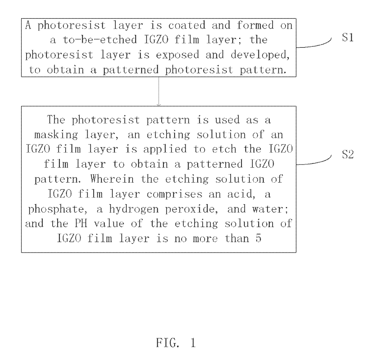
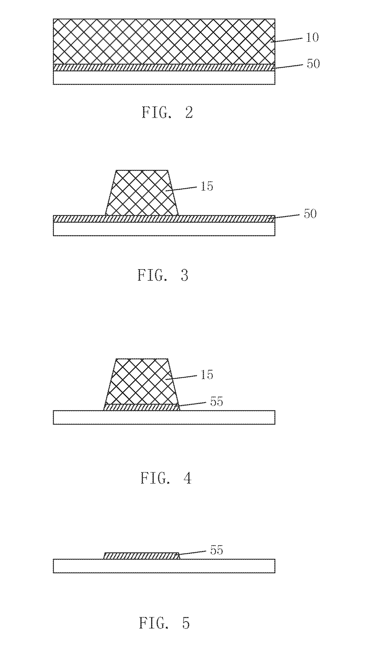
[0029]The present invention provides an etching solution of IGZO film layer, which comprises an acid, a phosphate, a hydrogen peroxide, and water. A PH value of the etching solution of IGZO film layer is no more than 5.

[0030]Among the etching solution of IGZO film layer, a mass percentage of the acid is 2% to 5%, a mass percentage of the phosphate is 5% to 10%, a mass percentage of the hydrogen peroxide is 15% to 22%, and rest is the water.

[0031]Specifically, the acid is a mixed acid of an inorganic acid and an organic acid.

[0032]Furthermore, the inorganic acid is phosphoric acid. The organic acid is selected from at least one from the group consisting of acetic acid, oxalic acid, and oxalic acid.

[0033]Specifically, the phosphate is selected from at least one from the group consisting of dihydrogen phosphate ...


PUM

PropertyMeasurementUnit
temperatureaaaaaaaaaa
PHaaaaaaaaaa
sizeaaaaaaaaaa

Abstract

The present invention provides an etching solution of IGZO film layer and an etching method of the same. The etching solution of IGZO film layer of the present invention comprises an acid, a phosphate, a hydrogen peroxide, and water; and the PH value of the etching solution of IGZO film layer is no more than 5, which are capable of effectively controlling the rate of the etching solution to make the etching rate uniform, then the IGZO film layer is etched stably without introducing impurities affecting the electric characteristic of the IGZO, to raise the stability of the IGZO-TFT device. The etching method of IGZO film layer, with applying the etching solution mentioned above, which is capable of effectively controlling the rate of the etching solution to make the etching rate uniform, then the IGZO film layer, is etched stably without introducing impurities affecting the electric characteristic of the IGZO, to raise the stability of the IGZO-TFT device.

Description

BACKGROUND OF THE INVENTIONField of Invention[0001]The present invention relates to the field of manufacturing the display panel, and more particularly to an etching solution of IGZO film layer and an etching method of the same.Description of Prior Art[0002]With the development of display technology, the liquid crystal display panel is gradually developed towards large-size and high-resolution, which means that the charging time of the pixel also becomes shorter and shorter, and the thin film transistor (TFTs) inside the display panel play an important role for pixel charging. However, the characteristic of the TFTs are mainly decided by the properties of the active layer. Conventional TFT devices usually use amorphous silicon (a-Si, AS) as an active layer. AS-TFT devices have been developed for a long time and the device characteristics are stable. However, the mobility of AS is low and its advantages are gradually lost under the development trend of high-resolution and high refres...

Claims


Application Information

Patent Timeline
Patent Type & Authority Applications(United States)
IPC IPC(8): C09K13/06H01L21/027H01L21/465H01L21/467H01L29/66H01L29/24H01L29/786H01L27/12
CPCC09K13/06H01L21/0274H01L21/465H01L21/467H01L29/66969H01L29/24H01L29/7869H01L27/127H01L27/1288H01L27/1225
Inventor GAN, QIMING
Owner SHENZHEN CHINA STAR OPTOELECTRONICS SEMICON DISPLAY TECH CO LTD
Features
  • R&D
  • Intellectual Property
  • Life Sciences
  • Materials
  • Tech Scout
  • Unparalleled Data Quality
  • Higher Quality Content
  • 60% Fewer Hallucinations
Learn More