Process window widening using coated parts in plasma etch processes

a plasma etching and process window technology, applied in the direction of basic electric elements, electrical equipment, electric discharge tubes, etc., can solve the problems of difficult to define small features and difficulty in patterning these devices, and achieve the effect of improving the patterning process, reducing the size, and reducing the difficulty of defining small features

Active Publication Date: 2019-02-07
APPLIED MATERIALS INC
View PDF4 Cites 12 Cited by
  • Summary
  • Abstract
  • Description
  • Claims
  • Application Information

AI Technical Summary

Benefits of technology

[0005]As semiconductor devices become smaller, patterning these devices may become more challenging. Smaller features may be harder to define. This may be a result of the decreased size or of more stringent tolerances needed for performance, reliability, and manufacturing throughput. The methods described below may provide an improved patterning process.
[0006]Flowing a mixture of plasma effluents and a gas by nickel plated materials may allow for etching at lower pressures. Lower pressure processing may be advantageous for smaller and deeper semiconductor features by facilitating etchants to travel to the bottom of a narrow and deep feature without contacting and etching a sidewall. Nickel plating may increase selectivity by maintaining a low etch amount of silicon at lower pressures. Without intending to be bound by theory, it is believed that nickel may scavenge fluorine radicals or hydrogen radicals, which may be responsible for undesired etching of silicon. Nickel may coat parts of the chamber that are downstream of significant mixing of gases and plasma etchants. Nickel and may coat all parts along the flow path of plasma effluents in the chamber downstream of mixing.

Problems solved by technology

As semiconductor devices become smaller, patterning these devices may become more challenging.
Smaller features may be harder to define.

Method used


Image

  • Process window widening using coated parts in plasma etch processes
  • Process window widening using coated parts in plasma etch processes
  • Process window widening using coated parts in plasma etch processes

Examples


Embodiment Construction

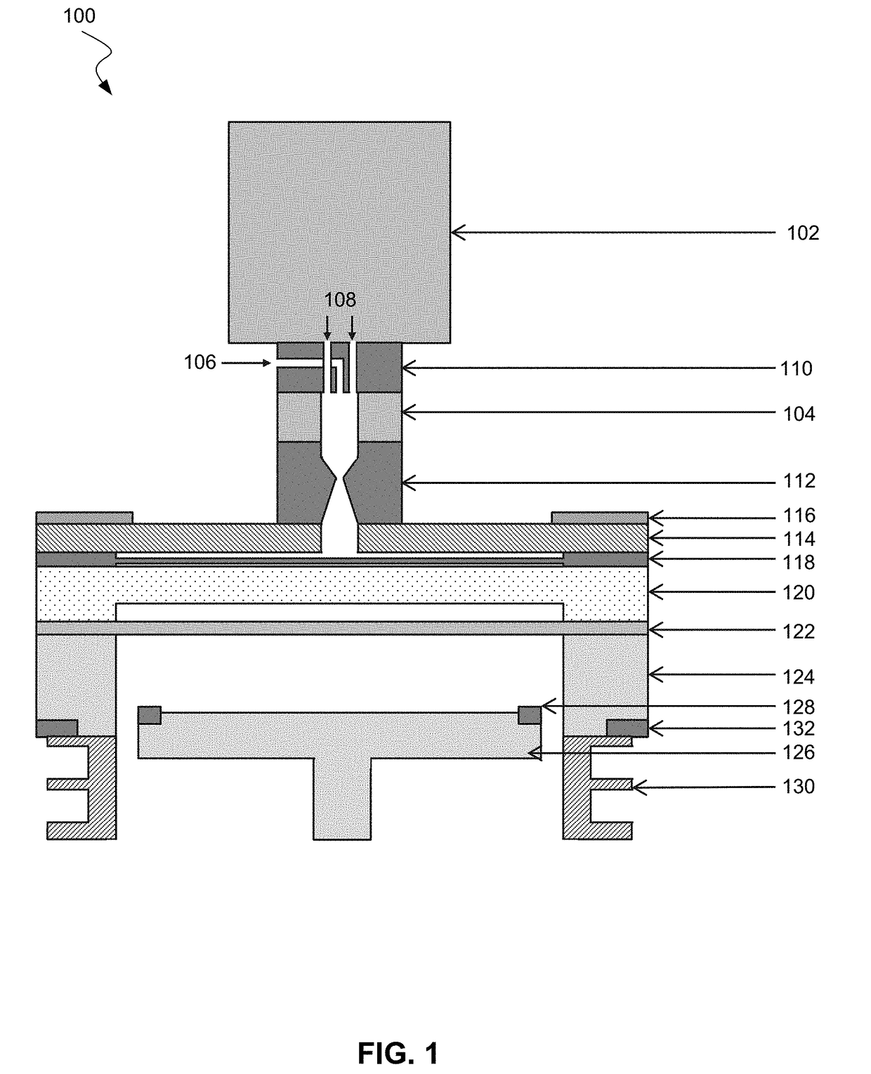
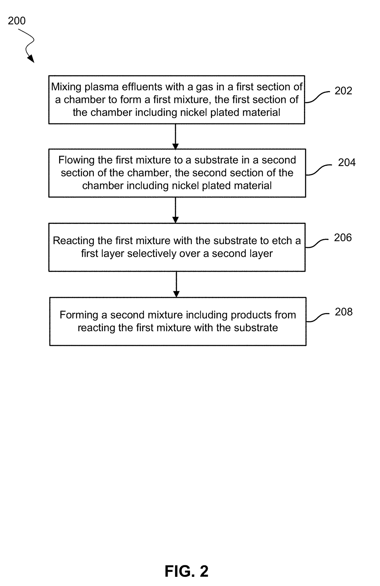
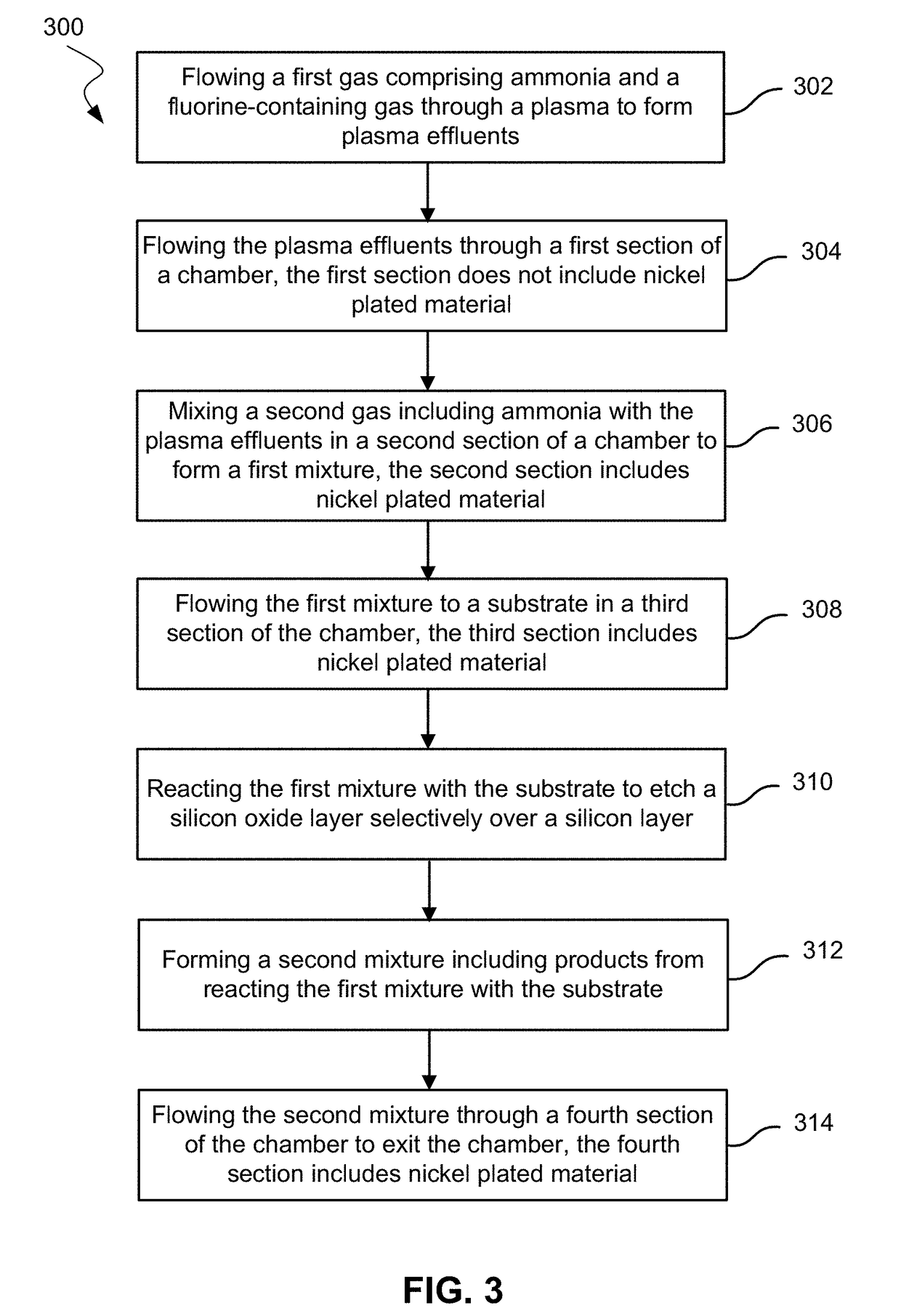
[0020]Conventional systems and methods for etching silicon oxide may not be suited for low pressures. Low pressures may be preferable for smaller and deeper semiconductor features. However, at lower pressures, etch selectivity may decrease. For example, during the etch of thermal oxide at lower pressures, the etch amount of thermal oxide may decrease, while the etch amount of silicon may increase. At low pressures, the density of reactive components, such as radicals, decreases. As a result, the etch rate of thermal oxide may decrease. Unreacted or incompletely reacted species may also be present in the chamber. At lower pressures, these unreacted species (e.g., fluorine radicals or hydrogen radicals) may react with silicon in the substrate, increasing the etch rate of silicon. Conventional methods etching at increased chamber pressure in order to react the radicals with the substrate or other gaseous species.

[0021]Embodiments of the present technology may allow for low pressure etc...


PUM


Abstract

Embodiments of the present technology may include a method of etching. The method may include mixing plasma effluents with a gas in a first section of a chamber to form a first mixture. The method may also include flowing the first mixture to a substrate in a second section of the chamber. The first section and the second section may include nickel plated material. The method may further include reacting the first mixture with the substrate to etch a first layer selectively over a second layer. In addition, the method may include forming a second mixture including products from reacting the first mixture with the substrate.

Description

TECHNICAL FIELD[0001]The present technology relates to semiconductor processes and equipment. More specifically, the present technology relates to improving process selectivity during low pressure etching operations.BACKGROUND[0002]Integrated circuits are made possible by processes which produce intricately patterned material layers on substrate surfaces. Producing patterned material on a substrate requires controlled methods for removal of exposed material. Chemical etching is used for a variety of purposes including transferring a pattern in photoresist into underlying layers, thinning layers, or thinning lateral dimensions of features already present on the surface. Often it is desirable to have an etch process that etches one material faster than another facilitating, for example, a pattern transfer process. Such an etch process is said to be selective to the first material. As a result of the diversity of materials, circuits, and processes, etch processes have been developed wi...

Claims


Application Information

Patent Timeline
Patent Type & Authority Applications(United States)
IPC IPC(8): H01L21/3065H01J37/32
CPCH01L21/3065H01J37/3244H01J37/32467H01L21/31053H01L21/02164H01L21/02123H01L21/02315H01L21/31116
Inventor YANG, DONGQINGTAN, TIEN FAKHILLMAN, PETERZHU, LALAINGLE, NITIN K.LUBOMIRSKY, DMITRYSNEDIGAR, CHRISTOPHERXIA, MING
Owner APPLIED MATERIALS INC
Why Eureka
Try Eureka