Imaging apparatus, imaging display system, and display apparatus

a technology of imaging display system and display apparatus, which is applied in the direction of instruments, semiconductor/solid-state device details, radiation controlled devices, etc., can solve the problems of image degradation and easy capture of light in the fiber optic pla

Inactive Publication Date: 2019-02-14
SONY CORP
View PDF3 Cites 2 Cited by
  • Summary
  • Abstract
  • Description
  • Claims
  • Application Information

AI Technical Summary

Benefits of technology

[0060]In the above-described imaging apparatus 1, the radioactive ray emitted from the source 300 enters the wavelength conversion layer 12, and thereafter, the wavelength conversion layer 12 outputs light (e.g. visible light). Thereafter, the light enters each device section 11A and then is converted into an electric signal by the photoelectric converter (photodiode PD). The electric signal is read out with from each device section 11A, transmitted to the wiring substrate 10, and then outputted to an external circuit. This makes it possible to detect the radioactive ray as the electric signal.

Problems solved by technology

However, with the technique disclosed in the above-described PTL 1, light is easily trapped in the fiber optic plate.
This reduces photosensitivity, which leads to image degradation.

Method used


Image

  • Imaging apparatus, imaging display system, and display apparatus
  • Imaging apparatus, imaging display system, and display apparatus
  • Imaging apparatus, imaging display system, and display apparatus

Examples


embodiment

[Configuration]

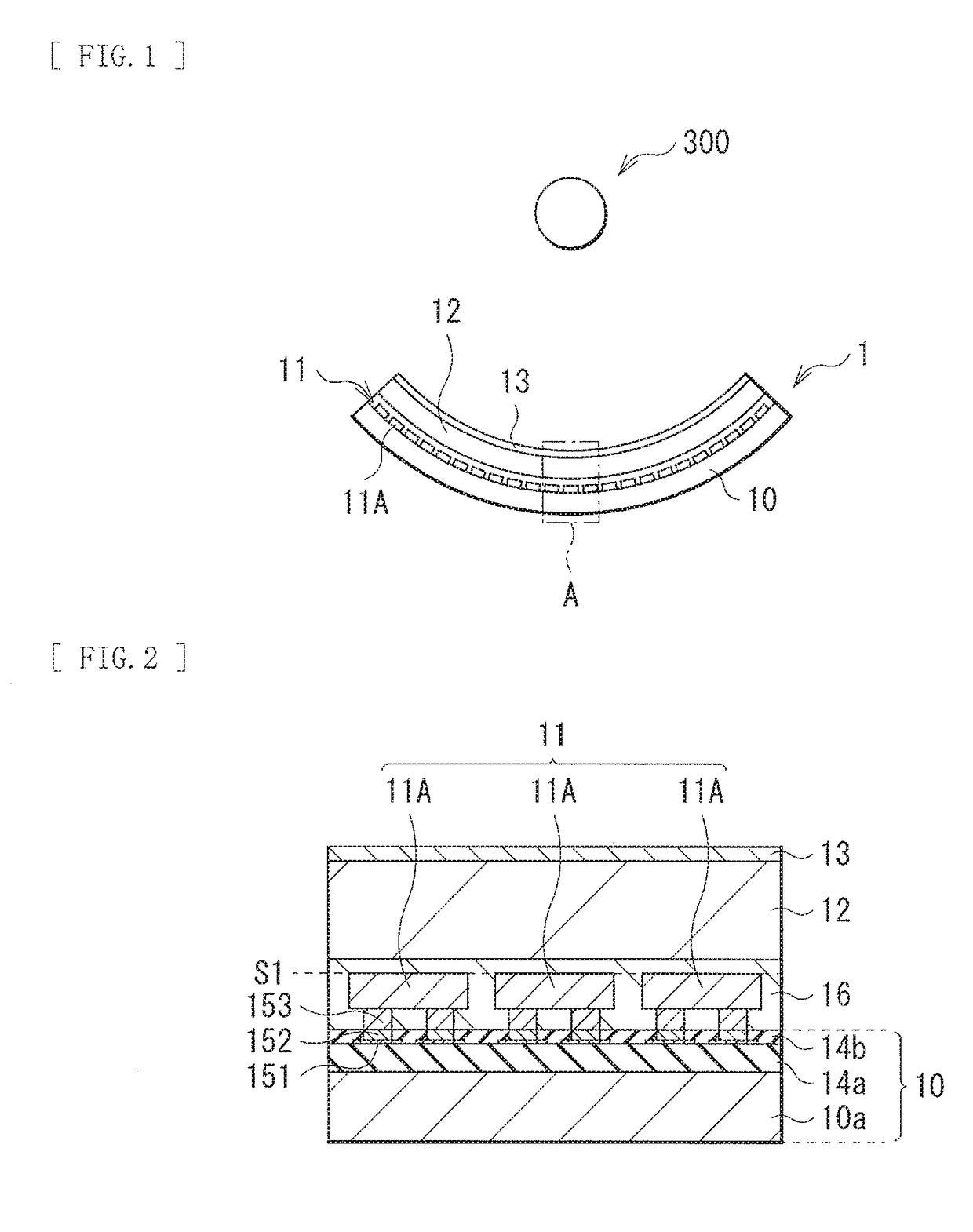
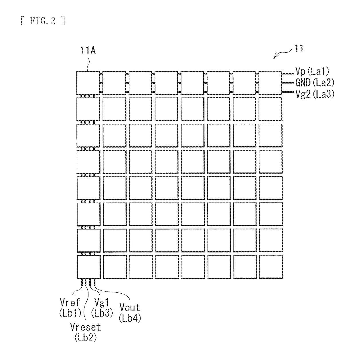
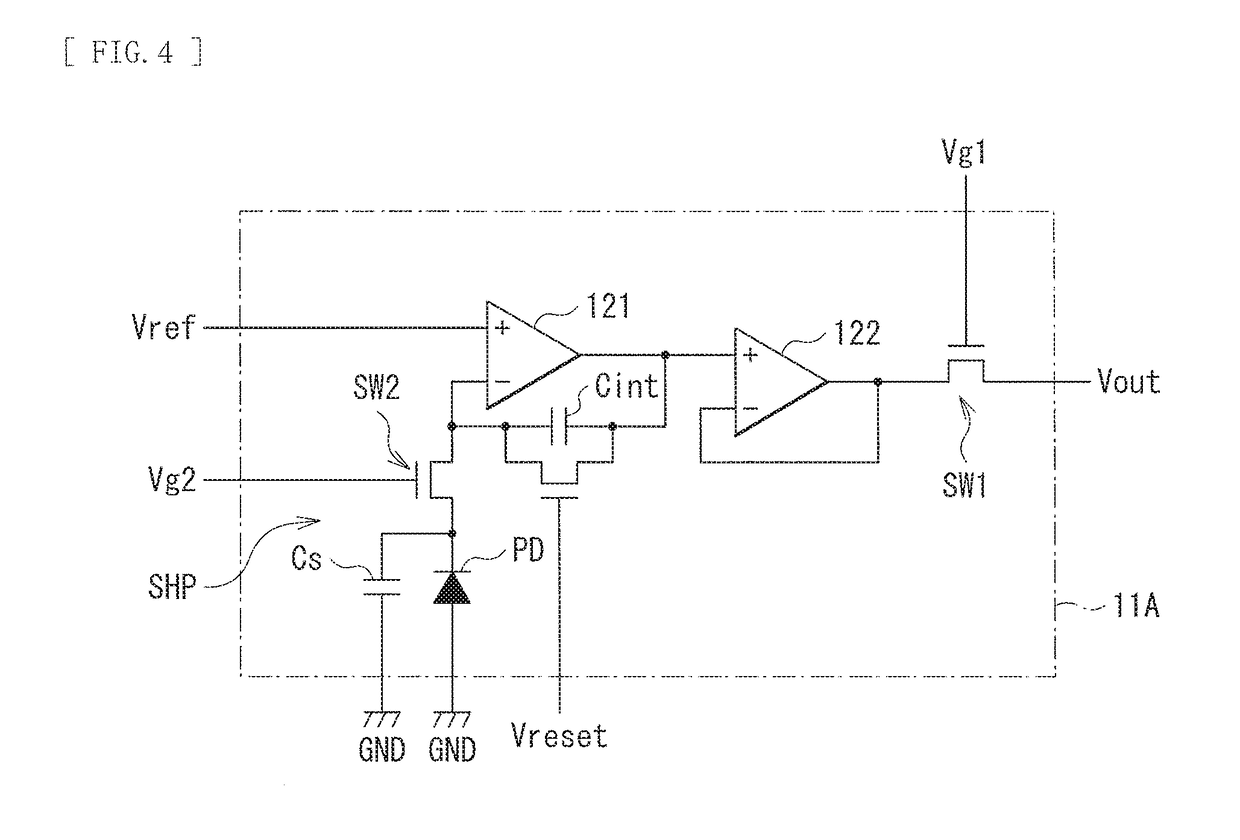
[0039]FIG. 1 illustrates an example of a cross-sectional configuration of an imaging apparatus (imaging apparatus 1) according to an embodiment of the present disclosure together with a radiation source (source 300). FIG. 2 is an enlargement of a region A that is a part of FIG. 1. The imaging apparatus 1 is a radiation detector that detects a radioactive ray such as an α-ray, β-ray, γ-ray, or an x-ray, and is, for example, an imaging apparatus of an indirect conversion system. The indirect conversion system means a system of converting a radioactive ray into an optical signal and then into an electric signal. The imaging apparatus 1 includes, for example, a pixel array section 11, a wavelength conversion layer 12, and a reflection layer 13 in this order on a wiring substrate 10.

[0040]The wiring substrate 10 includes, for example, a plurality of wiring layers (wiring layers 151) on a substrate 10a. The substrate 10a includes, for example, glass, silicon (Si), or an org...

modification example 1

[0071]FIG. 13 illustrates a functional configuration of an imaging apparatus (imaging apparatus 4) according to a modification example 1. Although description of the above-described embodiment involves the configuration in which the pixel array section 11 includes the active pixel circuit, in this modification example, the pixel array section 11 includes a so-called passive pixel circuit. The imaging apparatus 4 includes, for example, the pixel array section 11 and a driver that drives the pixel array section 11 on a substrate 410. The driver includes, for example, a row scanner 430, a horizontal selector 440, a column scanner 450, and a system controller 460.

[0072]In the pixel array section 11, like the above-described embodiment, the plurality of device sections 11A are disposed in a matrix. Pixel drive lines 470 extending in a row direction and vertical signal lines 480 extending in a column direction are coupled to the device sections 11A. The vertical signal lines 480 each tran...

application example

[0079]FIG. 15 illustrates an example of a functional configuration of an imaging display system (imaging display system 5) according to an application example. The imaging display system 5 includes, for example, the imaging apparatus 1 including the above-described pixel array section 11, an image processor 6, and a display apparatus 7. The image processor 6 performs predetermined image processing on an imaging signal Dout obtained by the imaging apparatus 1. The display apparatus 7 displays an image on the basis of the imaging signal Dout obtained by the imaging apparatus 4, and specifically displays an image based on the imaging signal processed by the image processor 6 (display signal D1).

[0080]In this embodiment, a component having passed through the object 400 of the radioactive ray emitted from the source 300 to an object 400 is detected by the imaging apparatus 1 to obtain the imaging signal Dout. The imaging signal Dout is inputted to the image processor 6 and is subjected t...


PUM


Abstract

An imaging apparatus includes: a substrate; and a plurality of device sections each including a photoelectric converter and disposed on the substrate to be spaced from one another and to collectively form a concave shape.

Description

TECHNICAL FIELD[0001]The present disclosure relates to an imaging apparatus, an imaging display system, and a display apparatus that detect a radioactive ray such as an α-ray, a β-ray, a γ-ray, or an x-ray.BACKGROUND ART[0002]Many imaging apparatuses applied to large FPDs (flat panel detectors) that image, for example, a chest, etc. employ amorphous silicon. With this imaging apparatus, which images an object while retaining a predetermined distance from a radiation source, sensitivity lowers in a periphery of an image to cause image degradation because the imaging apparatus is located away from the radiation source.[0003]Thus, for example, PTL 1 proposes a technique of suppressing resolution reduction as described above using a fiber optic plate having a processed surface shape.CITATION LISTPatent Literature[0004]PTL 1: Japanese Unexamined Patent Application Publication No. H09-112301SUMMARY OF THE INVENTION[0005]However, with the technique disclosed in the above-described PTL 1, l...

Claims


Application Information

Patent Timeline
Patent Type & Authority Applications(United States)
IPC IPC(8): G01T1/20H01L27/146H01L23/538
CPCG01T1/2018H01L27/14609H01L23/5387H01L27/14663H01L27/14636H01L27/14618H01L24/16H01L24/13H01L2224/16227H01L2224/13116H01L2224/13111H01L27/14629H01L21/4853H01L24/81H01L2224/81815H01L2224/81201H01L27/14685H01L25/0655H01L25/50H01L31/03762H01L27/14607H01L2924/181H01L2224/81203H01L2224/81444H01L2224/81455H01L2224/81469H01L2224/81801H04N25/70G01T1/20189G01T1/20187G01T1/20188H01L2924/00012H01L2924/00014H01L27/144H01L31/02H01L31/08H01L27/14H01L25/041
Inventor MATSUMOTO, KATSUJIYANAGAWA, SHUSAKUIGARASHI, TAKAHIROICHIKI, HIROSHI
Owner SONY CORP
Why Eureka
Try Eureka