Slot Waveguide with Structural Modulation

a waveguide and structural modulation technology, applied in waveguides, individually energised antenna arrays, instruments, etc., can solve the problems of large mode volume overlap with eo polymer, limit the maximum length of slow light waveguides, and reduce propagation loss, reduce propagation loss, and resist fabrication imperfections

Active Publication Date: 2019-02-28
OMEGA OPTICS
View PDF0 Cites 16 Cited by
  • Summary
  • Abstract
  • Description
  • Claims
  • Application Information

AI Technical Summary

Benefits of technology

[0009]In one respect, disclosed is a slow light slot waveguide with PC structure along the rails. Such a PC structure takes advantage of the strong mode confinement in the low-index region of a conventional slot waveguide together with the slow light enhancement from the PC structures. Its simple geometry makes it robust to fabrication imperfections and helps reduce the propagation loss, while still maintaining the benefits of large mode overlap and slow light enhancement. Using the structure as a phase shifter and converting the phase shift to amplitude modulation through a Mach-Zehnder interferometer (MZI) structure, an integrated silicon-organic hybrid EO modulator is disclosed. The observed effective EO coefficient is as high as 490 pm / V at 1562 nm wavelength. The measured half wave voltage and length product is 0.91 V. cm and may be further improved by adding narrow connecting arms. The disclosed structure offers a competitive, novel phase shifter design, which is simple, highly efficient and with low optical loss, for on-chip silicon-organic hybrid EO modulators.

Problems solved by technology

The slow light effect is frequently explored to extend the interaction duration, but the propagation loss is proportional to the slow down factor, which ultimately limits the maximum length of the slow light waveguide.
The bandwidths and modulation efficiencies in these modulators are therefore limited by the free carrier dynamics.
High modulation efficiencies have been achieved in slot waveguides because slot waveguides confine the optical mode in the low index slot region infiltrated with EO polymer material, which leads to large mode volume overlap with the EO polymer.
However, due to low poling efficiency in the narrow slot, the effective in-device EO coefficient is far away from its maximum potential value.
In a 2D slot PC waveguide, however, the optical loss in the slow light region and its robustness to fabrication variations, considering its complicated structure and delicate arrangement of the PC holes, is a concern, especially in a dispersion-engineered PC slot waveguide [X. Zhang, A. Hosseini, S. Chakravarty, J. Luo, A. K.-Y.

Method used


Image

  • Slot Waveguide with Structural Modulation
  • Slot Waveguide with Structural Modulation
  • Slot Waveguide with Structural Modulation

Examples


Embodiment Construction

Detailed Description of the Invention

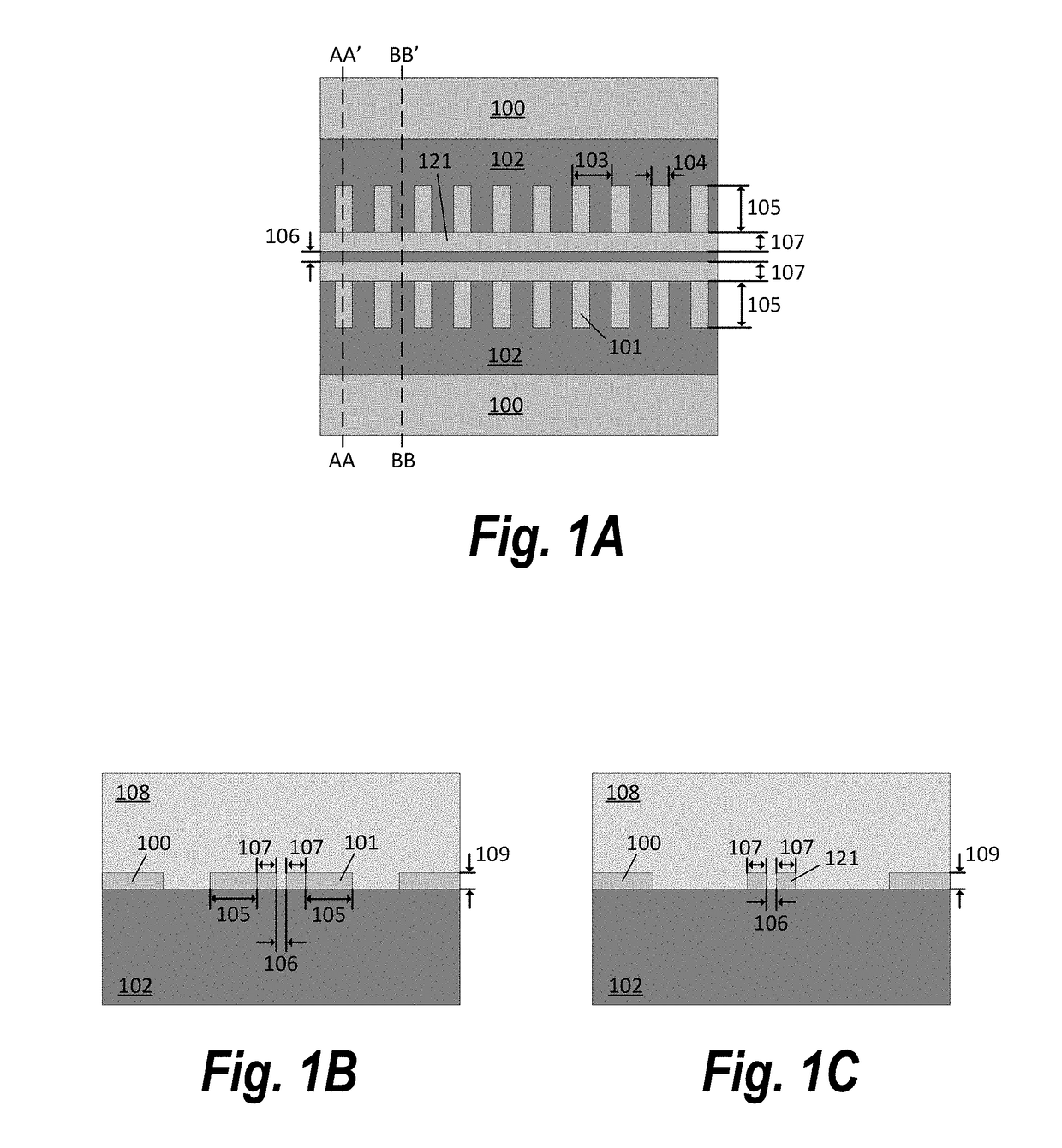
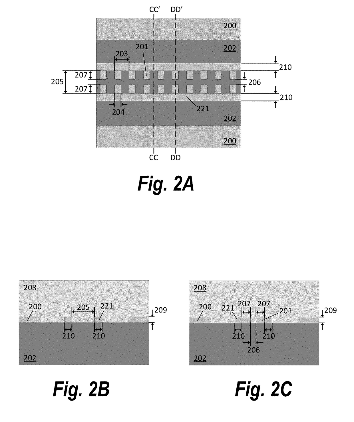
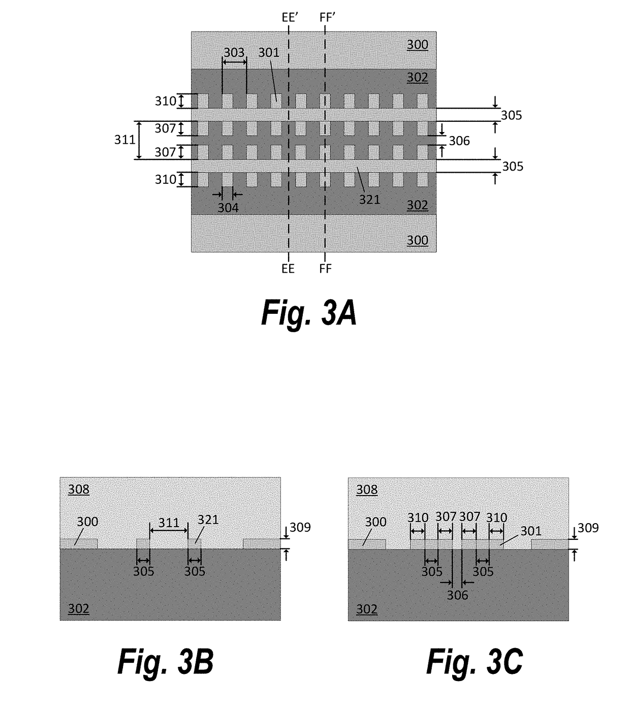
[0031]Detailed descriptions of the preferred embodiments are provided herein. It is to be understood, however, that the present invention may be embodied in various forms. The specific details disclosed herein are not to be interpreted as limiting, but rather as a basis for the claims and as representative basis for teaching one skilled in the art to employ the present invention in virtually any appropriately detailed system, structure, or manner. In all the accompanying drawings, same numerals are used within each figure to represent the same or similar materials, and redundant descriptions are omitted.

[0032]The present disclosure teaches methods and apparatuses to enhance the photon-matter interaction of conventional slot waveguides. The principle behind these methods and apparatuses may be summarized as introducing perturbations or defects into conventional slot or strip waveguides to slow down or trap photons. The present disclosure demonstra...


PUM


Abstract

Apparatuses for communication or sensing are disclosed, the apparatuses comprising a substrate; a bottom cladding disposed on the substrate; a device layer disposed on the bottom cladding, wherein the device layer comprises: two substantially parallel rails extending from an input side to an output side of the device layer and configured to form a slot between the two substantially parallel rails, wherein each of the two substantially parallel rails comprises an inner edge adjacent to the slot and an outer edge opposite the slot; and one or more teeth coupled to each of the two substantially parallel rails; and a top cladding disposed onto the device layer and bottom cladding; wherein the bottom cladding, the device layer, and the top cladding are configured to support at least one optical guided mode. Other embodiments are described and claimed.

Description

I. STATEMENT REGARDING FEDERALLY SPONSORED RESEARCH[0001]The U.S. Government has a paid-up license in this invention and the right in limited circumstances to require the patent owner to license others on reasonable terms as provided for by the terms of the contract DE-SC0013178 awarded by Department of Energy (DOE), the contract FA9550-16-C-0033 awarded by Air Force Office of Scientific Research, and the contract FA8650-15-M-5006 awarded by Air Force Research Laboratory.II. BACKGROUNDField of the Invention[0002]The present disclosure relates generally to the field of optical and sensing devices, and more specifically to an apparatus and method for optical communication, microwave communication, biological sensing, and chemical sensing.Background of the Invention[0003]The statements in this section merely provide background information related to the present disclosure and may not constitute prior art.[0004]In recent decades, integrated photonics has received considerable attention ...

Claims


Application Information

Patent Timeline
Patent Type & Authority Applications(United States)
IPC IPC(8): H01Q21/00H01Q21/22H01P3/123
CPCH01Q21/0062H01Q21/22H01P3/123G02B6/12007G02B2006/12138G02F2202/022G02B6/1225G02B6/1228G02F2202/32G02F1/065G02F1/011G01T1/24G02F1/00G02F1/3615H04B10/50
Inventor XU, XIAOCHUANCHEN, RAY T.
Owner OMEGA OPTICS
Why Eureka
Try Eureka