Regulator circuit

a regulator circuit and regulator technology, applied in the field of linear regulators, can solve the problems of reducing responsivity, reducing phase margin and gain margin, and difficult to maintain stability over a wide load range, and achieve the effect of reducing current consumption

Active Publication Date: 2019-03-14
ROHM CO LTD
View PDF8 Cites 8 Cited by
  • Summary
  • Abstract
  • Description
  • Claims
  • Application Information

AI Technical Summary

Benefits of technology

[0031]This arrangement is capable of automatically and seamlessly switching the load state between a heavy-load state in which the first error amplifier EA1 operates effectively and a light-load state in which the second error amplifier EA2 operates effectively with a given current ITH as a boundary thereof.
[0032]Also, by suspending the operation of the first error amplifie

Problems solved by technology

With the linear regulator 800 shown in FIG. 1, it is difficult to maintain stability over a wide load range.
Specifically, this arrangement has a problem of a reduction of the phase margin and gain margin in a part of the load range (or otherwise the entire load range).
In order to secure stability over the entire load range, this arrangement requires a tradeoff problem of reduced responsivity.
This becomes a cause of degradation of transient characteristics.
There is a delay time before the operation of the error

Method used


Image

  • Regulator circuit
  • Regulator circuit
  • Regulator circuit

Examples


first embodiment

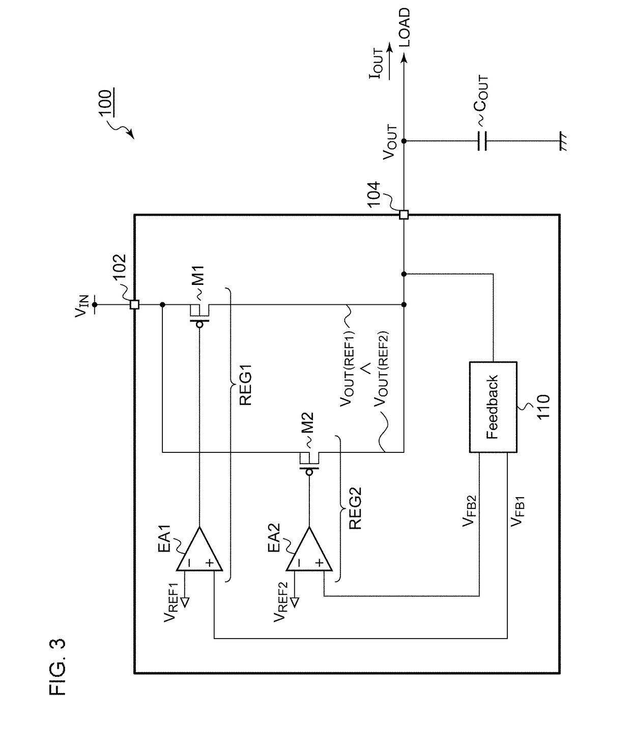
[0089]FIG. 3 is a circuit diagram showing a regulator circuit 100 according to a first embodiment. The regulator circuit 100 receives an input voltage VIN via its input terminal 102, and supplies an output voltage VOUT stabilized to a given target voltage VOUT(REF) to a load (not shown) coupled to an output terminal 104 thereof. The regulator circuit 100 is also referred to as an LDO (Low Drop Output) circuit. An output capacitor COUT is coupled to the output terminal 104 for smoothing the output voltage VOUT. The components of the regulator circuit 100 may be monolithically integrated on a single semiconductor substrate except for the output capacitor COUT.

[0090]The regulator circuit 100 includes a first transistor M1, a second transistor M2, a first error amplifier EA1, and a second error amplifier EA2. The first transistor M1 and the first error amplifier EA1 form a first linear regulator (heavy-load-supporting regulator) REG1 that is capable of supplying electric power to the lo...

example 1.1

[0107]FIG. 5 is a circuit diagram showing a regulator circuit 100A according to an example. With this example, the relations VFB1=VFB2, and VREF1>VREF2 hold true. A feedback circuit 110A includes resistors R1 and R2. The feedback ratio α1 of the first feedback signal VFB1 is equal to the feedback ratio α2 of the second feedback signal VFB2, which is represented by α=R2 / (R1+R2).

VFB1=VFB2=VOUT×α

[0108]The reference value VREF2 employed by the second error amplifier EA2 is higher than the reference value VREF1 employed by the first error amplifier EA1. A reference voltage source 120 generates a predetermined reference voltage VREF. The reference voltage VREF is supplied without change to the first error amplifier EA1, which is used as the first reference value VREF1. Furthermore, a positive offset voltage ΔV is added to the reference voltage VREF so as to generate the second reference voltage VREF2.

[0109]Alternatively, the reference voltage VREF may be used as the second reference volta...

example 1.2

[0112]FIG. 7 is a circuit diagram showing a regulator circuit 100B according to an example. With the regulator circuit 100B, a designed reference value VOFS is applied to the second error amplifier EA2. By applying such an input offset voltage VOFS2, an effective reference value VREF2 is shifted. From another viewpoint, by applying such an input offset voltage VOFS2, it can be understood that the effective second feedback signal VFB2 is shifted.

[0113]The first error amplifier EA1 adjusts the gate voltage of the first transistor M1 such that the relation VREF=VFB holds true. On the other hand, the second error amplifier EA2 adjusts the gate voltage of the second transistor M2 such that the relation VREF+VOFS2=VFB holds true.

[0114]Accordingly, the following relations hold true.

VOUT(REF1)=VREF×(R1+R2) / R2

VOUT(REF2)=(VREF+VOFS2)×(R1+R2) / R2

[0115]Thus, the following relation holds true.

VOUT(REF2)>VOUT(REF1)

[0116]Instead of or in addition to applying the input offset voltage VOFS2 to th...


PUM


Abstract

A regulator circuit supplies an output voltage VOUT to a load. A second transistor is arranged in parallel with a first transistor, and has a relatively small size. A feedback circuit generates a first feedback signal and a second feedback signal according to the output voltage VOUT. A first error amplifier controls the first transistor such that the first feedback signal approaches a first reference value. A second error amplifier controls the second transistor such that the second feedback signal approaches a second reference value. In a light-load state, the operation of the first error amplifier is maintained.

Description

BACKGROUND OF THE INVENTION1. Field of the Invention[0001]The present invention relates to a linear regulator.2. Description of the Related Art[0002]In various kinds of electronic circuits and electronic devices, a linear regulator is employed, configured to stabilize a DC voltage having a given voltage value to a DC voltage having a different voltage value. FIG. 1 is a circuit diagram showing a linear regulator. A linear regulator 800 receives a DC voltage VIN via an input terminal 802, and generates and outputs, via an output terminal 804, an output voltage VOUT stabilized to a predetermined target voltage VOUT(REF). The linear regulator 800 mainly includes an output transistor 806, an error amplifier 808, and a feedback circuit 810.[0003]The output transistor 806 is arranged between the input terminal 802 and the output terminal 804. The feedback circuit 810 divides the output voltage VOUT, and generates a feedback voltage VFB that corresponds to the output voltage VOUT. The erro...

Claims


Application Information

Patent Timeline
IPC IPC(8): G05F1/575G05F1/46H03K5/24
CPCG05F1/575G05F1/461H03K5/2472G05F3/262
Inventor YASUSAKA, MAKOTOINOUE, HIROKI
Owner ROHM CO LTD
Why Eureka
Try Eureka