Smart defect calibration system and the method thereof

a defect calibration and defect technology, applied in semiconductor/solid-state device testing/measurement, instruments, image enhancement, etc., can solve the problems of inaccurate critical area analysis, inaccurate judgment of killer defect/non-killer defect, and inaccuracy of defect size, so as to achieve accurate killer defect index, more accurate calibration, and high accuracy. the effect of defect size valu

Active Publication Date: 2019-03-21
ELITETECH TECH
View PDF0 Cites 12 Cited by
  • Summary
  • Abstract
  • Description
  • Claims
  • Application Information

AI Technical Summary

Benefits of technology

[0008]The main purpose of the invention is to Use the IC design layout and Critical Area Analysis method. In terms of the deviation value generated from the defect inspection tool, this invention provides input the coordinate deviation calibration value and the Calibration Factor for the defect size that can correct the coordinate deviation and defect size deviation of the defect data from the defect inspection tool. Combining the IC design layout data, the system overlaps the plurality of defect pattern to the mapped plurality of defect layout pattern one by one. Then, the system analyzes with Critical Area Analysis method to create the Killer Defect Index (KDI). This invention utilizes the precisely calibrated coordinate, the defect layout pattern, and the higher accurate calibrated defect size value. So, a more precise killer defect index can be generated with calibrated coordinate deviation calibration and defect size deviation calibration. When judging a defect relating to short circuit or open circuit failure probability, the defect failure result is more accurate and less incorrect judgment. This new invention will become an important tool that can identify a defect belonging to a killer defect category or a non-killer defect category.

Problems solved by technology

The inaccurate defect size issue is caused by the minimum metrology unit in the defect inspection tool.
This defect size deviation creates inaccurate Critical Area Analysis and correct killer defect / non-killer defect judgment.

Method used


Image

  • Smart defect calibration system and the method thereof
  • Smart defect calibration system and the method thereof
  • Smart defect calibration system and the method thereof

Examples


Embodiment Construction

[0035]In semiconductor wafer fab, semiconductor assembly fab, flat panel display fab, solar panel fab, printed circuit board fab, mask fab, LED fab or LED assembly fab, there must be run through mask, lithography, etching, and film deposition, etc. equipment and processing method to form a specific functioning product. Because there are many complex process steps in the manufacturing procedures, the process and equipment parameter control, equipment parameter shift, or technical bottleneck can produce the defects that would impact yield. Generation of those defects is inevitable. So in the manufacturing procedures of a semiconductor fab, fab team would always execute defect inspection and analysis to improve yield and reduce cost.

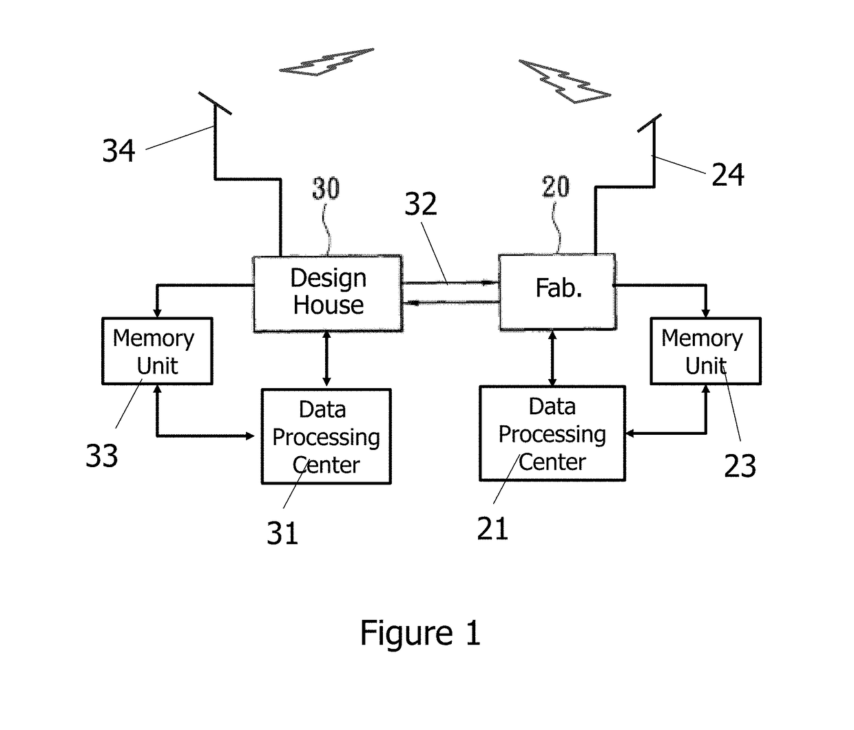
[0036]First of all, please review FIG. 1. It is an operation architecture chart for the present invention that involves a Smart Semiconductor Defect Calibration, Classification, and Sampling System and The Method Thereof. As shown in FIG. 1, a practice exam...


PUM

PropertyMeasurementUnit
defect sizeaaaaaaaaaa
geometry sizeaaaaaaaaaa

Abstract

The present invention relates to a Smart Defect Calibration, Diagnosis, Sampling System and The Method Thereof for manufacturing fab is provided. The intelligent defect diagnosis method comprises: receiving pluralities of defect data, design layout data, analyzing the defect data, design layouts, by a Critical Area Analysis (CAA) system, wherein the analyzing step further contains the sub-steps: superposing the defect contour pattern and the design layout, performing CAA to identify a killer or non-killer defect based on the open or short failure probability, defects are classified as high, medium, low, or negligible risk defect based on the Killer Defect Index, defect signal parameters, selecting defect samples based on the defect classification data, selecting alarm defect and filtering false defect with pattern match with defect pattern library and frequent failure defect library, performing coordinate conversion and pattern match between image contour and design layout for coordinate correction, creating a CAA accuracy correction system and defect size calibration system by analyzing original defect size data and defect contour size from image analysis, evaluating the defect size using measurement uncertainty analysis with statistical analysis methods to reach the purposes of increasing CAA accuracy and Killer Defect identification rate.

Description

BACKGROUND OF THE INVENTION1. Field of the Invention[0001]The present invention involves a Smart Semiconductor Defect Calibration, Classification, and Sampling System and The Method Thereof. Especially it is a Smart Defect Calibration, Classification, and Sampling System and The Method Thereof applied to the semiconductor manufacturing fab, semiconductor assembly fab, flat panel display manufacturing fab, solar panel manufacturing fab, printed circuit board manufacturing fab, mask manufacturing fab, LED fab or assembly fab.2. Description of the Prior Art[0002]In general, the manufacturing of integrated circuit wafer in a semiconductor fab includes processing with mask, lithography process, etching (plasma etch and wet etch), film deposition, Cu dual damascene process, chemical mechanical polishing, and multi-patterning exposure processes and equipment. During the manufacturing stage, the random defect and systematic defect are normally created due to such factors as the equipment's ...

Claims


Application Information

Patent Timeline
Patent Type & Authority Applications(United States)
IPC IPC(8): G01N21/95H01L21/66G06F17/50G06T7/00
CPCG01N21/9501H01L22/12G06F17/5081G06T7/001G06F17/504G06T2207/30148G01N21/8851G01N2021/8861G01N2021/8864G01N2021/8874H01L22/20G06F30/398G06F30/3323
Inventor LEU, IYUN
Owner ELITETECH TECH
Why Eureka
Try Eureka