
Method for manufacturing semiconductor device

Active Publication Date: 2019-03-28
TOYODA GOSEI CO LTD
View PDF15 Cites 3 Cited by
  • Summary
  • Abstract
  • Description
  • Claims
  • Application Information

AI Technical Summary

Benefits of technology

This patent describes a method for manufacturing a semiconductor device by creating a first groove in a stacked body made of gallium nitride layers and depositing a p-type impurity on the side and bottom of the groove. The p-type impurity is then ion-implemented into the first semiconductor layer to form a p-type semiconductor region in the groove. This helps to compensate for any highly concentrated impurities in the device and improves its breakdown resistance. Overall, this method ensures the efficient and reliable production of semiconductor devices.

Problems solved by technology

This complicates the manufacturing process of the semiconductor device, and foreign matter might enter the semiconductor layers in the manufacturing process.
However, in the case of ion-implanting a p-type impurity into a gallium nitride (GaN)-based semiconductor, it is difficult to ion-implant the p-type impurity into a deep position.
The above-described p-type pillar layer is unfortunately difficult to form.
Therefore, it is difficult for the above-described technique disclosed in JP2009-141243A to compensate for the n-type semiconductor region of the high concentration.

Method used


Image

  • Method for manufacturing semiconductor device
  • Method for manufacturing semiconductor device
  • Method for manufacturing semiconductor device

Examples


first embodiment

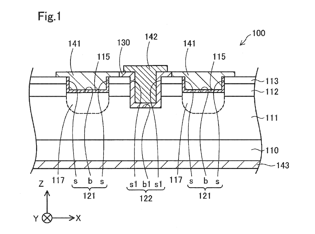
[0040]FIG. 1 is a schematic diagram illustrating part of a semiconductor device 100 in cross section. It should be noted that FIG. 1 and the following schematic diagrams are provided to clarify technical features of the semiconductor device 100 and are not intended for indicating dimensions of each component accurately. For ease of description, XYZ axes substantially orthogonal to one another are illustrated in FIG. 1. The XYZ axes in FIG. 1 correspond to XYZ axes in other drawings. It should be noted that in the following description, a +Z-axis direction side will be also referred to as “above” or “upper side”.

[0041]The semiconductor device 100 is a gallium nitride (GaN)-based semiconductor device. According to this embodiment, the semiconductor device 100 is a vertical trench metal-oxide-semiconductor field-effect transistor (MOSFET). For example, the semiconductor device 100 is used for power control and is also called power device.

[0042]The semiconductor device 100 includes a su...

second embodiment

[0083]FIG. 13 is a schematic diagram illustrating part of a semiconductor device 200 according to a second embodiment in cross section. The semiconductor device 200 includes a p-type semiconductor layer 116 stacked on each of the p-type impurity deposition regions 115. The p-type semiconductor layer 116 is a structure formed by selective growth of a gallium nitride (GaN)-based semiconductor on the p-type impurity deposition region 115. According to this embodiment, the p-type semiconductor layer 116 contains magnesium (Mg) as an acceptor element. According to this embodiment, the p-type semiconductor layer 116 has a concentration of magnesium (Mg) equal to or less than 4E18 cm−3. According to this embodiment, the p-type semiconductor layer 116 has a thickness equal to or larger than 1 nm and equal to or less than 10 nm. The other configuration of the semiconductor device 200 is substantially the same as the semiconductor device 100 according to the first embodiment, and therefore wi...

modification 1

[0086]According to the above-described embodiments, the p-type impurity is deposited on the side portions “s” and the bottom portions “b” of the first grooves 121 by delta-doping. However, sputtering or vapor deposition may be adopted to deposit the p-type impurity on the side portions and the bottom portions “b” of the first grooves 121. An oxide film containing the p-type impurity may be formed on the side portions “s” and the bottom portions “b” of the first grooves 121.


PUM


Abstract

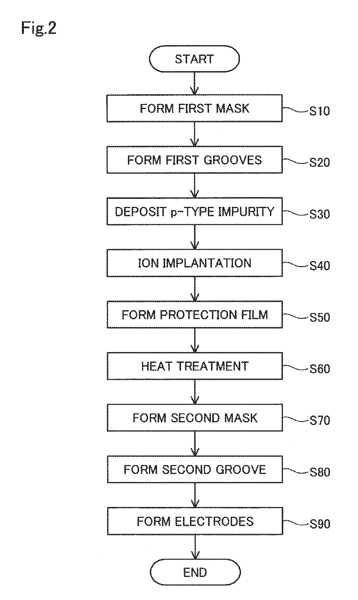
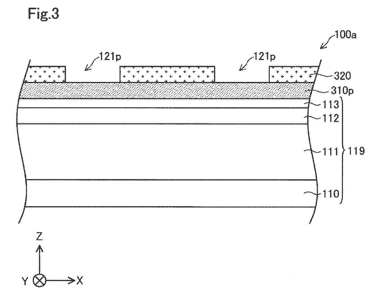
A method for manufacturing a semiconductor device comprises forming first groove, depositing, and ion-implanting. At the step of forming the first groove, the first groove is formed in a stacked body comprising a gallium nitride (GaN)-based first semiconductor layer containing an n-type impurity and a gallium nitride (GaN)-based second semiconductor layer stacked on the first semiconductor layer and containing a p-type impurity. The first groove has a bottom portion located in the second semiconductor layer. At the depositing step, a p-type impurity is deposited on side portion and the bottom portion of the first groove. At the ion-implanting step, a p-type impurity is ion-implanted into the first semiconductor layer through the first groove.

Description

CROSS-REFERENCE TO RELATED APPLICATION[0001]The present application claims priority from Japanese patent application No. 2017-187563 filed on Sep. 28, 2017, the entirety of disclosures of which is hereby incorporated by reference into this application.BACKGROUNDField[0002]The present disclosure relates to a method for manufacturing a semiconductor device utilizing ion implantation.Related Art[0003]In a semiconductor device made of a gallium nitride (GaN)-based semiconductor, a technique has been known in which a p-type semiconductor region is formed by ion implantation to relax electric field concentration that occurs when a voltage is applied.[0004]JP2015-138958A discloses a technique of: forming a recess in a first semiconductor layer formed by epitaxial growth; ion-implanting a p-type impurity into the bottom of this recess to form a field relaxing layer; and regrowing a second semiconductor layer on the field relaxing layer and the surface of the first semiconductor layer by epi...

Claims


Application Information

Patent Timeline
IPC IPC(8): H01L29/06H01L29/20H01L29/78H01L21/306H01L21/308H01L21/02H01L21/265H01L21/266H01L21/285H01L21/28H01L29/66
CPCH01L29/0634H01L29/2003H01L29/7813H01L21/30621H01L21/308H01L21/0254H01L21/02579H01L21/02584H01L21/0262H01L21/26546H01L21/266H01L21/28575H01L21/28264H01L29/66515H01L29/66734H01L21/02458H01L21/02494H01L29/41766H01L29/1095H01L21/26553
Inventor NIWA, TAKAKIFUJII, TAKAHIROKOSAKI, MASAYOSHI
Owner TOYODA GOSEI CO LTD
Learn More