Microwave antenna apparatus, packing and manufacturing method

a microwave antenna and microwave antenna technology, applied in the direction of waveguide horns, non-resonant long antennas, semiconductor/solid-state device details, etc., can solve the problems of narrow operating bandwidth (1-5%), distorted radiation patterns, and high amount of parasitic radiation to all directions, so as to achieve easy manufacturing and cost-saving effect of effect of effect of radiation efficiency

Active Publication Date: 2019-04-18
SONY CORP
View PDF5 Cites 22 Cited by
  • Summary
  • Abstract
  • Description
  • Claims
  • Application Information

AI Technical Summary

Benefits of technology

[0005]It is an object to provide a microwave antenna apparatus and a microwave antenna package, which are radiation efficient and can be manufactured easier ...

Problems solved by technology

The disadvantage of the aforementioned solutions are their narrow operating bandwidth (1-5%), distorted radiation patterns due to thick mold compound in the radiating direction, and the high amount of parasitic radiation to all directions.
Further, these plan...

Method used


Image

  • Microwave antenna apparatus, packing and manufacturing method
  • Microwave antenna apparatus, packing and manufacturing method
  • Microwave antenna apparatus, packing and manufacturing method

Examples


embodiment 5

6. Microwave antenna apparatus as defined in embodiment 5,

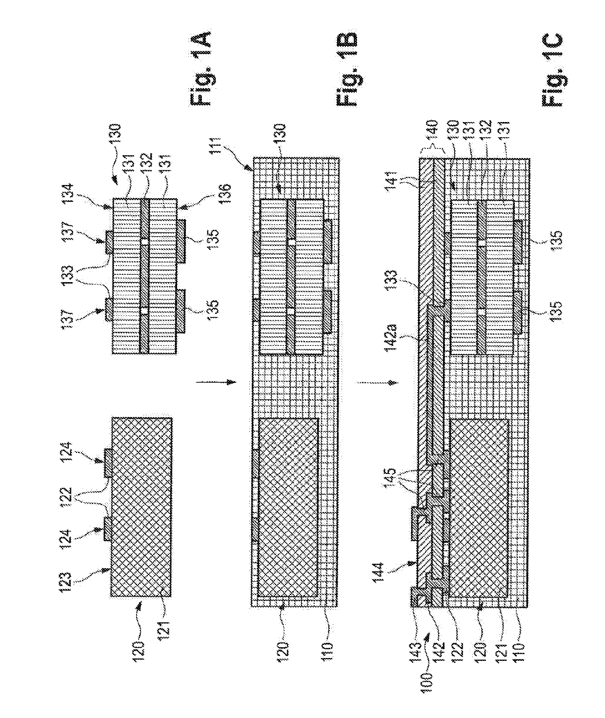
wherein the antenna element (430) comprises one or more connection lines (431) connecting one or more antenna feed lines (133) with the radiating element (135) through the substrate layer (131).

embodiment 6

7. Microwave antenna apparatus as defined in embodiment 6,

wherein the antenna element (430) comprises one or more parasitic elements (432) arranged within the antenna substrate layer (131) between the ground layer (132) arranged within the antenna substrate layer (131) and one or more antenna feed lines (133).

8. Microwave antenna apparatus as defined in embodiment 6 or 7,

wherein the antenna element (530) comprises one or more connection lines (531) connecting one or more antenna feed lines (133) with the radiating element (135) through the substrate layer (131) and one or more vias (532) connecting the metal layer (142) with the antenna element (135).

9. Microwave antenna apparatus as defined in any preceding embodiment,

wherein the ground layer (132) is arranged on the second surface (136) of the antenna substrate layer (131) and the radiating element (135) is arranged in the redistribution layer (140) and is in contact with the metal layer (142).

10. Microwave antenna apparatus as de...


PUM


Abstract

A microwave antenna apparatus comprises a semiconductor element and an antenna element embedded into a mold layer, which is covered by a redistribution layer. The antenna element is preferably configured as SMD component so that it can be handled by a standard pick and place process. The coupling between semiconductor element and antenna element is provided either by a metal layer or aperture coupling within the redistribution layer. The microwave antenna apparatus may be coupled to a PCB arrangement thus forming an embedded wafer-level ball grid array (eWLB) or embedded micro-wafer-level-packaging (emWLP) package.

Description

BACKGROUNDField of the Disclosure[0001]The present disclosure relates to a microwave antenna apparatus, a microwave antenna package and a method of manufacturing a microwave antenna apparatus.Description of Related Art[0002]Fan-out wafer level packaging technology such as the embedded wafer-level ball grid array (eWLB) has matured for microwave and mm-wave radar and communication systems over the past years. This packaging technology is the first choice for low-cost system integration of MMICs, passives, and antennas into a single plastic type package. Many different types of planar antenna structures in fan-out wafer level packages have been published, e.g. in M. Wojnowski et al., “Embedded Wafer Level Ball Grid Array (eWLB) Technology for Millimeter-Wave Applications,” Proc. IEEE 13th Electronics Packaging Technology Conference (EPTC2011), Singapore, pp. 423-429, December 2011. They all have in common, that the antenna elements are printed on one or more redistribution layers (RDL...

Claims


Application Information

Patent Timeline
IPC IPC(8): H01P5/107H01Q1/22H01Q11/08H01Q15/00H01Q9/04H01Q9/27
CPCH01P5/107H01Q1/2283H01Q11/08H01Q15/006H01Q9/0457H01Q9/0485H01Q9/27H01L2223/6677H01L2224/04105H01L2224/12105H01L2224/18H01L2224/96H01Q9/42H01L23/66H01Q13/02
Inventor KHAN, WASIF TANVEERTOPAK, ALI ERAYOTT, ARNDT THOMAS
Owner SONY CORP
Why Eureka
Try Eureka