Artificial Synapse with Hafnium Oxide-Based Ferroelectric Layer in CMOS Back-End

a ferroelectric layer and back-end technology, applied in the direction of metallic oxides, semiconductor devices, capacitors, etc., can solve the problem of challenging implementation on the silicon complementary metal-oxide-semiconductor (cmos) platform

Active Publication Date: 2019-05-02
IBM CORP
View PDF0 Cites 6 Cited by
  • Summary
  • Abstract
  • Description
  • Claims
  • Application Information

AI Technical Summary

Benefits of technology

[0005]The present invention provides artificial synaptic devices with a hafnium oxide (HfO2)-based ferroelectric layer that can be implemented in the complementary metal-oxide-semiconductor (CMOS) back-end. In one aspect of the invention, an artificial synapse element is provided. The artificial synapse element in...

Problems solved by technology

However, implementation on a silicon complementary metal-oxide-semiconductor (CMOS) platform remains challenging due to incompatibilities of perovskite ferroelectrics with CMOS proces...

Method used


Image

  • Artificial Synapse with Hafnium Oxide-Based Ferroelectric Layer in CMOS Back-End
  • Artificial Synapse with Hafnium Oxide-Based Ferroelectric Layer in CMOS Back-End
  • Artificial Synapse with Hafnium Oxide-Based Ferroelectric Layer in CMOS Back-End

Examples


Embodiment Construction

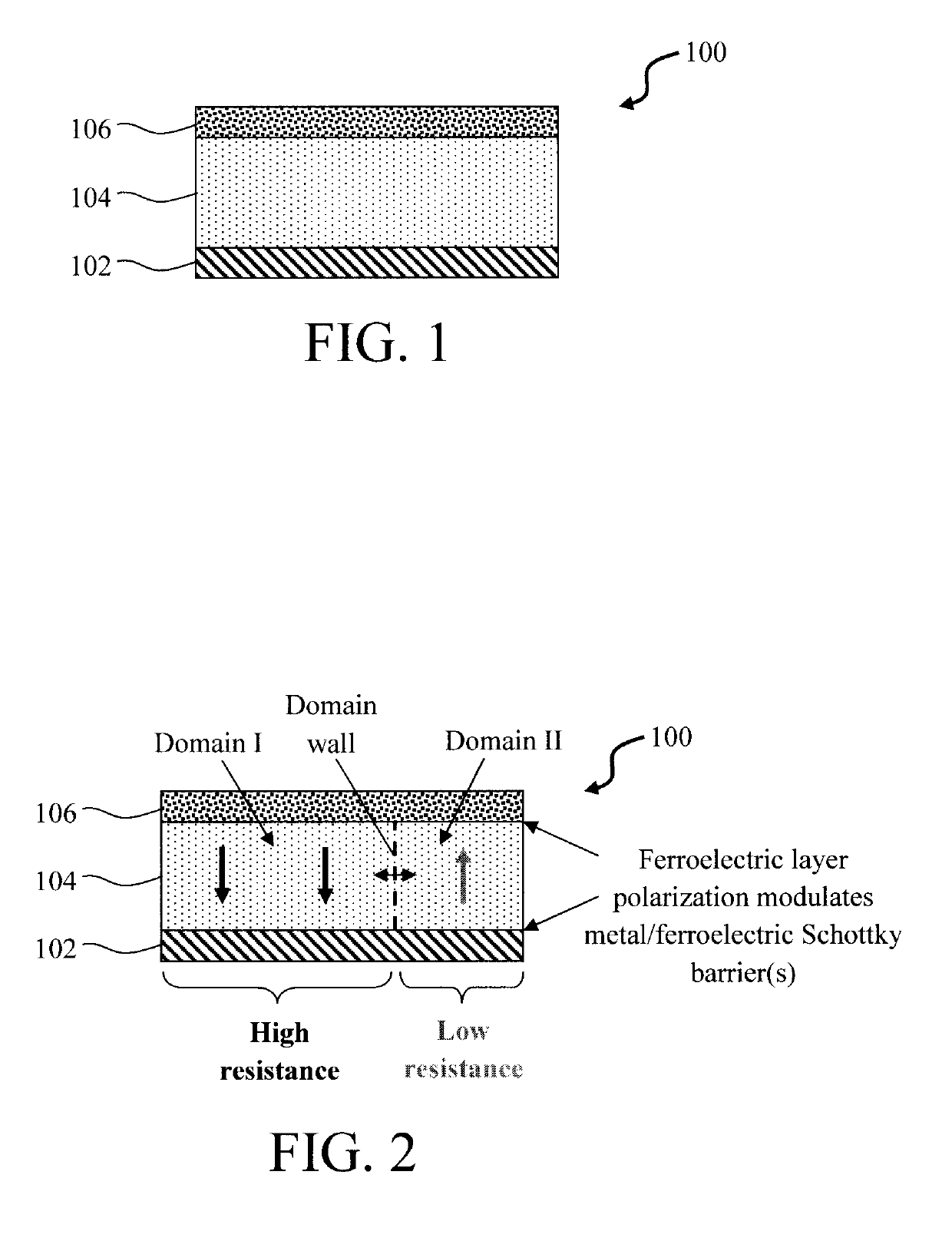
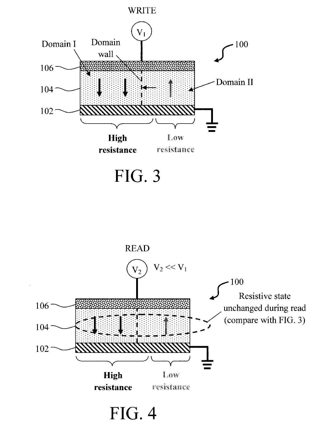
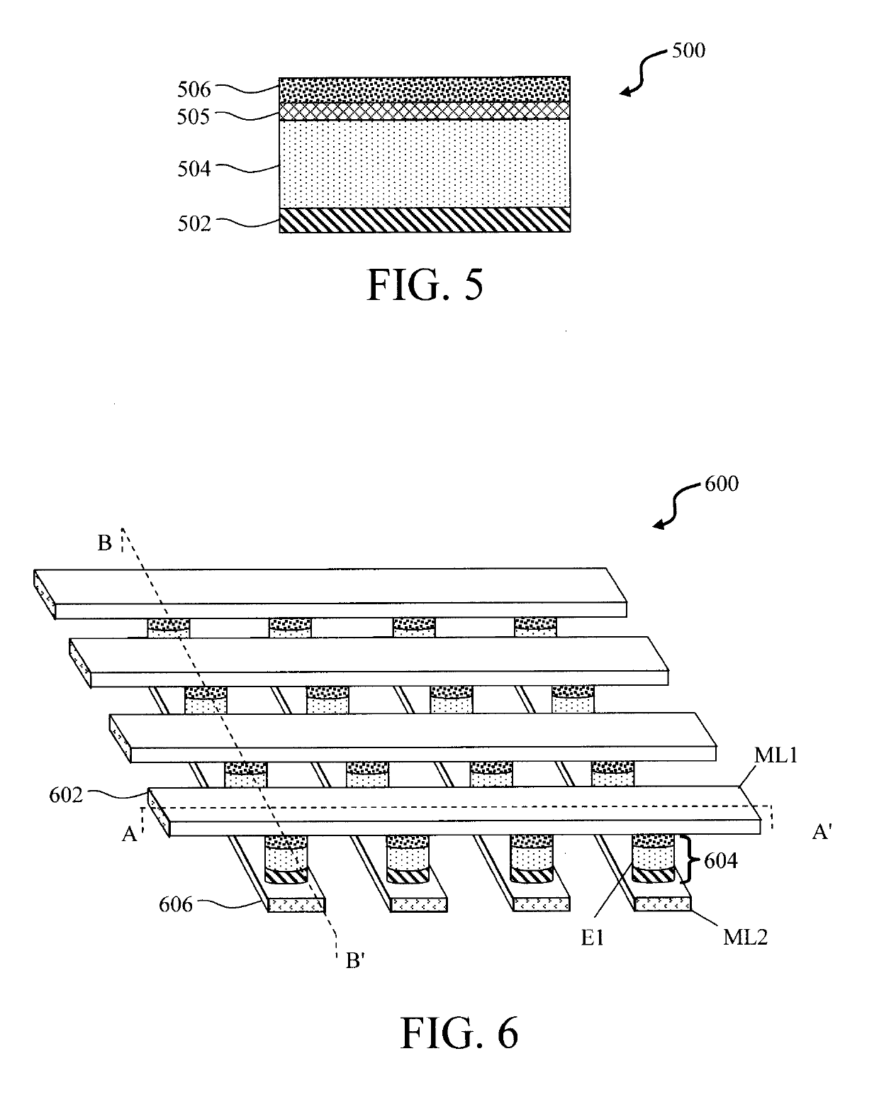
[0028]Provided herein are ferroelectric artificial synapse devices that can be implemented in the complementary metal-oxide-semiconductor (CMOS) back-end, i.e., over a layer of CMOS driver circuitry. Namely, an artificial synapse is described herein that includes a metal-ferroelectric-metal (MFM) or metal-ferroelectric-semiconductor (MFS) stack in the CMOS back-end-of-line (BEOL) that incorporates a hafnium oxide (HfO2)-based ferroelectric material that crystallizes at temperatures not exceeding the maximum allowed back-end-of-line temperature (TBEOL).

[0029]By way of example only, the TBEOL is less than or equal to about 450° C., and preferably less than or equal to about 400° C. Temperatures in excess of these values can damage or degrade the performance of the existing circuitry including the back-end CMOS driver circuitry.

[0030]FIG. 1 is a diagram illustrating an exemplary artificial synapse element 100 in accordance with the present techniques. As shown in FIG. 1, artificial syn...


PUM


Abstract

Artificial synaptic devices with an HfO2-based ferroelectric layer that can be implemented in the CMOS back-end are provided. In one aspect, an artificial synapse element is provided. The artificial synapse element includes: a bottom electrode; a ferroelectric layer disposed on the bottom electrode, wherein the ferroelectric layer includes an HfO2-based material that crystallizes in a ferroelectric phase at a temperature of less than or equal to about 400° C.; and a top electrode disposed on the bottom electrode. An artificial synaptic device including the present artificial synapse element and methods for formation thereof are also provided.

Description

FIELD OF THE INVENTION[0001]The present invention relates to artificial synaptic devices, and more particularly, to artificial synaptic devices with a hafnium oxide (HfO2)-based ferroelectric layer that can be implemented in the complementary metal-oxide-semiconductor (CMOS) back-end.BACKGROUND OF THE INVENTION[0002]The realization of a synaptic element is of interest for hardware implementation of deep learning networks. Weights are modified and stored by modulating the conductivity of non-volatile memory array elements. Use of the adjustable channel conductance of ferroelectric (FE) field-effect transistors (FETs) FE-FETs as a synaptic weight date back to the early 1990s. See H. Ishiwara, “Proposal of Adaptive-Learning Neuron Circuits with Ferroelectric Analog-Memory Weights,” Jpn. J. Appl. Phys. 32, 442-446 (January 1993).[0003]Significant progress has been made using perovskite ferroelectrics such as Pb(Zr,Ti)O3. See, for example, Kaneko et al., “Ferroelectric Artificial Synapse...

Claims


Application Information

Patent Timeline
IPC IPC(8): H01L49/02H01L27/11507H01B3/10H01L21/02H01L21/283H01L21/3213
CPCH01L28/40H01L27/11507H01L28/60H01B3/10H01L21/02181H01L21/02356H01L21/283H01L21/32133H01L28/55H10B63/80H10N70/20H10N70/826H10N70/8833H10N70/063H10B53/30
Inventor FRANK, MARTIN M.ANDO, TAKASHISUN, XIAOHAN, JIN PINGNARAYANAN, VIJAY
Owner IBM CORP
Why Eureka
Try Eureka