

Solder bump correction method
a technology of bump correction and soldering, which is applied in the direction of soldering apparatus, semiconductor/solid-state device details, manufacturing tools, etc., can solve the problem that the bumps that correspond to a fine circuit pattern cannot be formed, the separation limit is lower than the one at which printing can be performed, and the soldering cannot be performed on electronic components made of ceramics or the like without any treatment, etc. problem, to achieve the effect of uniform height, constant thickness and correcting the bumps
- Summary
- Abstract
- Description
- Claims
- Application Information
AI Technical Summary
Benefits of technology
Problems solved by technology
Method used
Image

Examples
Embodiment Construction
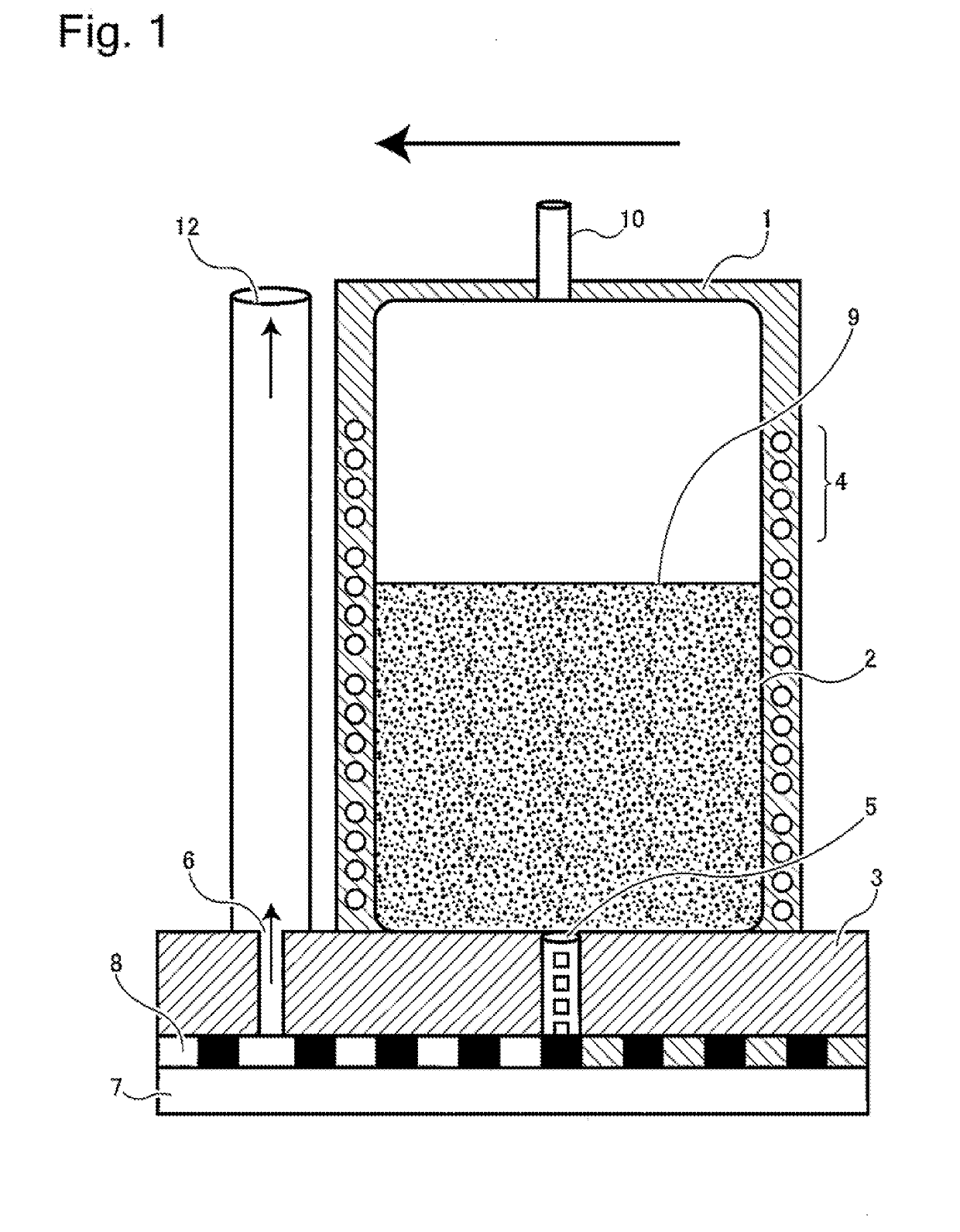
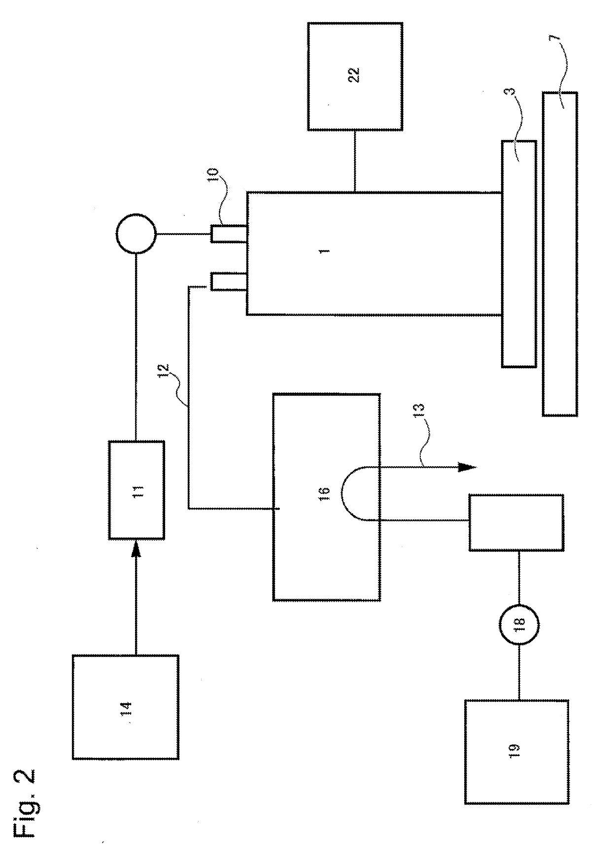
[0019]A configuration of a correction device according to one embodiment of the present invention is described. FIG. 1 is a view showing a head unit 1 of the correction device according to one embodiment of the present invention. FIG. 2 is a schematic view showing a schematic configuration of the correction device according to one embodiment of the present invention. The head unit 1 includes: a tank 2 which can store molten solder or the like; and a correction head 3 which is provided on a lower end of the head unit 1. When a fluid which requires a temperature control, such as molten solder, is used, a heating means may be mounted on the fluid tank 2. For example, a heater 4 may be wound around a middle portion of the fluid tank 2. The correction head 3 has a correction nozzle 5 and a suction port 6 which are provided at a lower end of the head. The suction port 6 is formed in the correction head 3 such that a suction step can be performed prior to a step performed by the correction...
PUM
| Property | Measurement | Unit |
|---|---|---|
| pressure | aaaaa | aaaaa |
| pressure | aaaaa | aaaaa |
| width | aaaaa | aaaaa |
Abstract
Description
Claims
Application Information