Synaptic crossbar memory array

a technology of memory array and crossbar, which is applied in the direction of digital storage, semiconductor/solid-state device details, instruments, etc., can solve the problems of reducing cell accuracy, requiring a very high degree of integration, and very low drive power,

Active Publication Date: 2019-05-30
IBM CORP
View PDF13 Cites 5 Cited by
  • Summary
  • Abstract
  • Description
  • Claims
  • Application Information

AI Technical Summary

Benefits of technology

[0006]Another feature of the invention is a synaptic crossbar memory array with a wid

Problems solved by technology

Making massive parallelism for these electronic synapses feasible requires a very high degree of integration coupled with very low drive power.
Unfortunately, the resist

Method used


Image

  • Synaptic crossbar memory array
  • Synaptic crossbar memory array
  • Synaptic crossbar memory array

Examples


Embodiment Construction

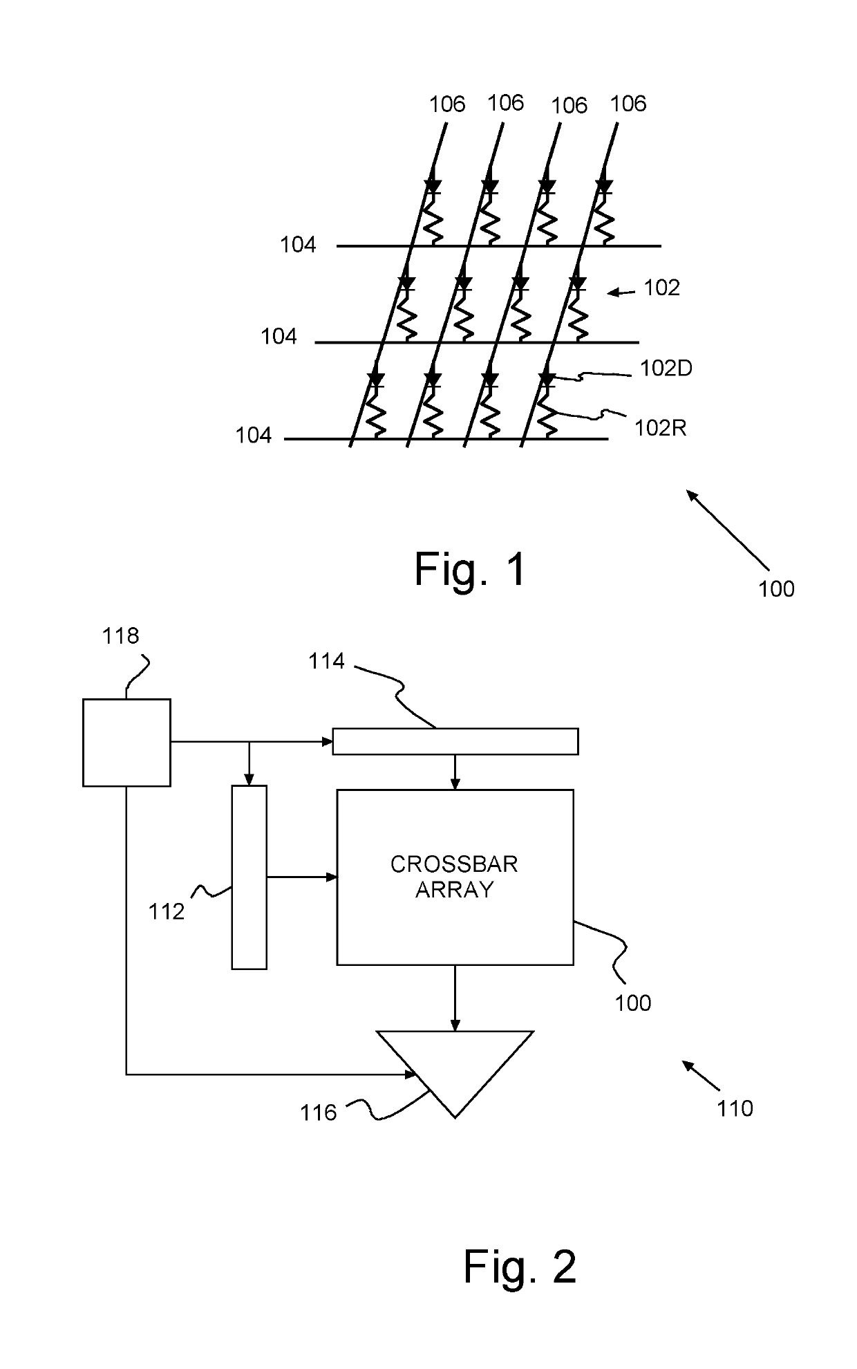
[0016]Turning now to the drawings and more particularly FIG. 1 shows a schematic example of a preferred synaptic crossbar or crosspoint memory array 100 of preferred electronic synapses 102, according to preferred embodiments of the present invention. The array 100 includes multiple lower electrode lines 104 in one direction, e.g., they direction, and multiple upper electrode lines 106 in an orthogonal direction, e.g., the x direction, and an electronic synapse 102 at each intersection of the electrode lines 104, 106.

[0017]Each synapse 102 includes a resistor 102R with one-time-alterable resistance in series with a diode 102D, and between a lower electrode line 104 and an upper electrode line 106. Each alterable resistor 102R of this example may be defined for at least two resistive states. The resistor 102R states include a first, un-altered or initial resistance state and a second, altered resistance state. Joule heating to alters the resistance, switching the resistor 102R from t...


PUM


Abstract

A method of forming an Integrated Circuit (IC) chip, the IC chip and an on-chip synaptic crossbar memory array. Chip devices are formed on a surface of a semiconductor wafer. A connective layer is formed above the chip devices. A bottom electrode layer is formed on the connective layer. A neuromorphic synapse layer is formed above the bottom electrode layer with each synapse on a bottom electrode. Upper electrodes are formed above the synapses and orthogonal to bottom electrode lines. Each synapse being beneath an upper electrode where the upper electrode crosses a bottom electrode. Upper electrodes are refractory metal and the bottom electrodes are copper, or vice versa.

Description

BACKGROUNDField of the Invention[0001]The present invention is related to Integrated Circuit (IC) chip manufacturing and particularly to manufacturing IC chips with an on-chip crossbar synapse array.Background Description[0002]Neuromorphic computing, which uses electronic synapses to mimic neuro-biological architectures present in the nervous system, recently has attracted a lot of interest. These electronic synapses have provided error tolerant, massive parallelism easing inputting complex information. Making massive parallelism for these electronic synapses feasible requires a very high degree of integration coupled with very low drive power.[0003]Typical state of the art neuromorphic synapses are metal oxide-based resistive switching devices. Unfortunately, the resistance of these resistive switching devices has been highly variable. The degree of variation degrades cell accuracy, degrading neuromorphic devices and system reliability.[0004]Thus, there is a need for reliable neuro...

Claims


Application Information

Patent Timeline
IPC IPC(8): G11C11/54H01L27/24H01L23/528G11C13/00H01L45/00H01L23/532H01L23/522
CPCG11C11/54H01L27/2436H01L23/528G11C13/0004H01L45/1233H01L45/1608H01L45/148H01L23/53257H01L23/53228H01L45/1666H01L23/5226H01L45/126H01L45/06G11C13/0069H01L27/2463G11C2213/52G11C17/165G11C2213/72H10B63/30H10N70/20H10N70/884H10N70/021H10N70/061H10B63/80H10N70/231H10N70/826H10N70/8413
Inventor AFZALI-ARDAKANI, ALIGERSHON, TALIA S.HASHEMI, POUYAHEKMATSHOARTABARI, BAHMAN
Owner IBM CORP
Why Eureka
Try Eureka