Check patentability & draft patents in minutes with Patsnap Eureka AI!

High speed memory interface

a memory interface and high-speed technology, applied in the field of communication, can solve the problems of scalability barriers, high cost, and inability to provide this density and quantity of interconnection wires between planar chip devices

Active Publication Date: 2019-06-13
KANDOU LABS
View PDF0 Cites 3 Cited by
  • Summary
  • Abstract
  • Description
  • Claims
  • Application Information

AI Technical Summary

Benefits of technology

The patent text describes a memory interface that allows for faster data transfer with fewer physical wires. This results in lower costs and reduced signal density, which can make it easier to connect the memory with graphics processing units (GPUs) and dynamic random access memory (DRAM) chips. Overall, the technology allows for higher bandwidth and improved performance.

Problems solved by technology

Although achievable using technologies such as a silicon interposer, providing this density and quantity of interconnection wires between planar chip devices is expensive.
Moreover, this number of connections to a controller device such as a GPU uses significant I / O pad “beachfront” on the controller die, creating a scalability barrier to future system requirements for two or more HBM connections to provide greater memory bandwidth or larger total memory size.

Method used


Image

  • High speed memory interface
  • High speed memory interface
  • High speed memory interface

Examples


example embodiment

[0281]FIGS. 12-23 show block diagrams of one representative implementation of the previously-described third EHBM embodiment, provided for descriptive purposes without implying limitation.

[0282]FIG. 12 is a block diagram of one embodiment of a Host Interface EHBM PHY.

[0283]FIG. 13 is a block diagram of one embodiment of a Base Chip EHBM PHY.

[0284]FIG. 14 is a block diagram of one embodiment of the HEI Command / Address pipeline operating in the Host to memory direction. In this example, all DFI signals are assumed to be synchronous to the MC clock, and FEC generation is internal to the SERDES.

[0285]FIG. 15 is a block diagram of one embodiment of the BEI Command / Address pipeline operating in the Host to memory direction. In this example the FEC check bit is internal to the SERDES, but the correction stage is external.

[0286]FIG. 16 is a block diagram of one embodiment of the BEI Command / Address pipeline operating in the memory to Host direction. In this example, FEC generation is intern...


PUM


Abstract

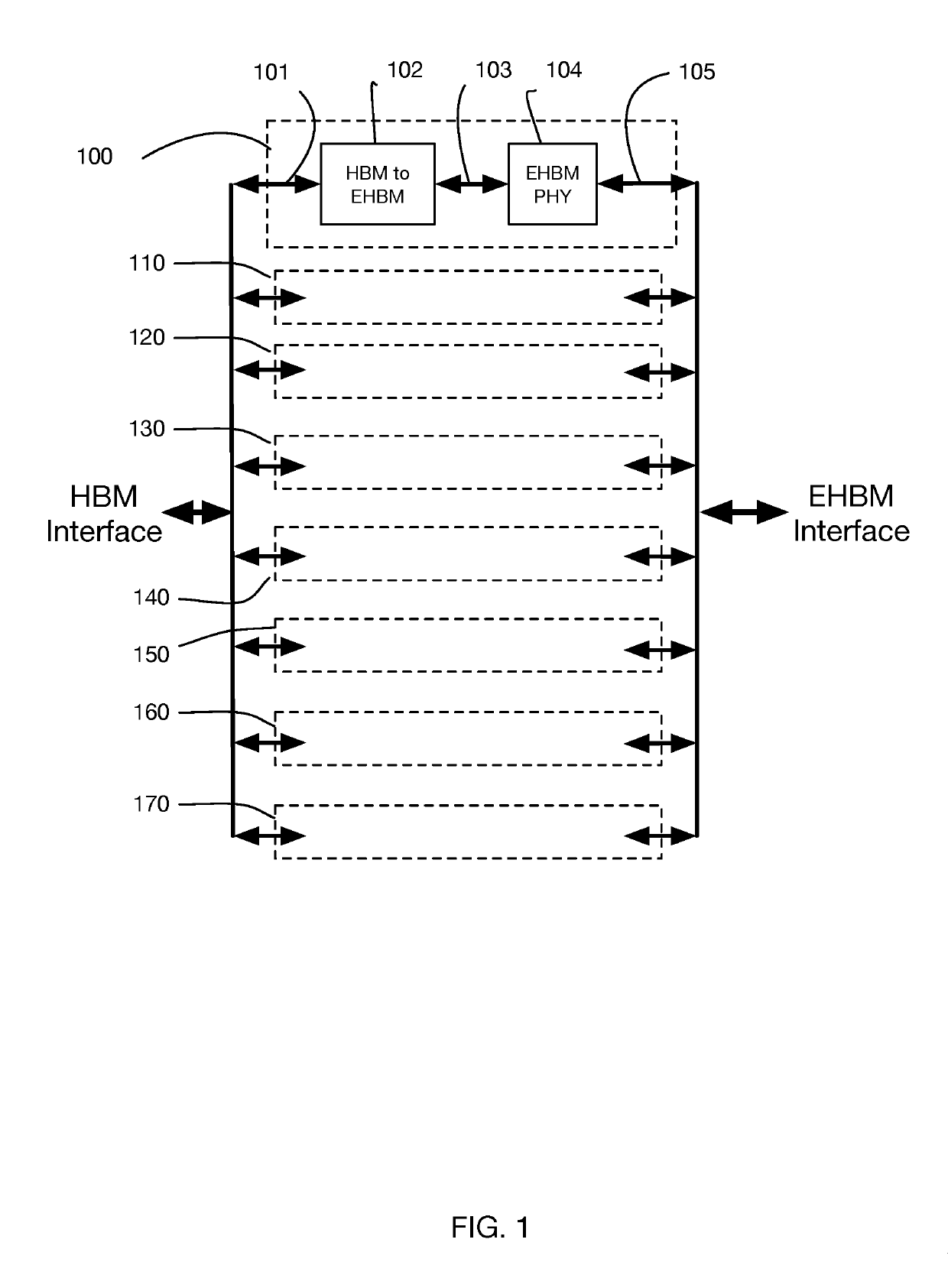
Systems and methods for an Enhanced High Bandwidth Memory (EHBM) are described, utilizing fewer physical wires than a HBM interface with each wire operating at a much higher signaling rate. The same logical signals and commands of HBM are supported over this higher-speed transport, with the resulting lower wire count and reduced signal density allowing use of lower-cost interconnection such as an organic rather than a silicon interposer between GPU and DRAM stack.

Description

REFERENCES[0001]The following references are herein incorporated by reference in their entirety for all purposes:[0002]U.S. Patent Publication No. 2011 / 0268225 of U.S. patent application Ser. No. 12 / 784,414, filed May 20, 2010, naming Harm Cronie and Amin Shokrollahi, entitled “Orthogonal Differential Vector Signaling”, hereinafter identified as [Cronie I];[0003]U.S. patent application Ser. No. 13 / 030,027, filed Feb. 17, 2011, naming Harm Cronie, Amin Shokrollahi and Armin Tajalli, entitled “Methods and Systems for Noise Resilient, Pin-Efficient and Low Power Communications with Sparse Signaling Codes”, hereinafter identified as [Cronie II];[0004]U.S. patent application Ser. No. 14 / 158,452, filed Jan. 17, 2014, naming John Fox, Brian Holden, Peter Hunt, John D Keay, Amin Shokrollahi, Richard Simpson, Anant Singh, Andrew Kevin John Stewart, and Giuseppe Surace, entitled “Chip-to-Chip Communication with Reduced SSO Noise”, hereinafter identified as [Fox I];[0005]U.S. patent applicatio...

Claims


Application Information

Patent Timeline
IPC IPC(8): G06F13/42G06F13/16G11C5/06G06F11/10
CPCG06F13/4243G06F13/1689G11C5/06G06F11/1004G06F1/08G06F13/161G06F13/1673G11C7/1006G11C7/1057G11C7/106G11C7/1078G11C7/1087G11C11/4093G06F1/06G06T1/60H04L1/00
Inventor SHOKROLLAHI, AMINHOLDEN, BRIANSTAUFFER, DAVID
Owner KANDOU LABS
Features
  • R&D
  • Intellectual Property
  • Life Sciences
  • Materials
  • Tech Scout
  • Unparalleled Data Quality
  • Higher Quality Content
  • 60% Fewer Hallucinations
Learn More