Photodiode device monolithically integrating waveguide element with photodiode element type of optical waveguide

a technology of optical waveguide and photodiode element, which is applied in the direction of optical waveguide light guide, optical element, instrument, etc., can solve the problems of complex modulation, large temperature dependence of pd commercially available in the field, and high cost. , to achieve the effect of avoiding time constant, high speed operation and high speed operation

Active Publication Date: 2019-09-05
SUMITOMO ELECTRIC DEVICE INNOVATIONS
View PDF7 Cites 3 Cited by
  • Summary
  • Abstract
  • Description
  • Claims
  • Application Information

AI Technical Summary

Problems solved by technology

However, a PD commercially available in the field often shows large temperature dependence, especially in optical sensitivity thereof, in the L-band.
Also, a future optical communication system inevitably requests a high speed operation exceeding 400 Gb / s and a complex modulation configuration such as multi-level amplitude modulation combined with a phase modulation.
However, a thinned absorption layer to shorten the carrier transport time inevitably increases the capacitance thereof to increase the time constant.

Method used


Image

  • Photodiode device monolithically integrating waveguide element with photodiode element type of optical waveguide
  • Photodiode device monolithically integrating waveguide element with photodiode element type of optical waveguide
  • Photodiode device monolithically integrating waveguide element with photodiode element type of optical waveguide

Examples


first modification

[0056

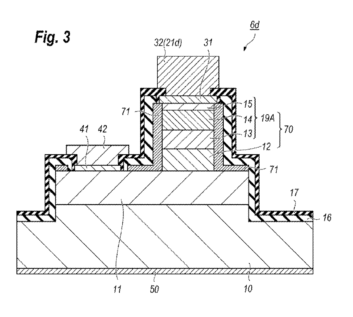
[0057]FIG. 12 is a cross sectional view of another PD device 2B that includes another PD element 6d and another waveguide element 8f, where FIG. 12 is taken along the line IV-IV indicated in FIG. 4. Both elements, 6d and 8f, are modified from the PD element 6d and the waveguide element 8f shown in FIG. 4. The arrangement of the PD device 2B shown in FIG. 12 has a feature that the PD device 2B omits the buffer layer 12 common to the PD element 6d and the waveguide element 8f but further provides an intermediate layer 18 in the PD element 6d. Other arrangements are substantially same with those shown in FIG. 4.

[0058]The PD element 6d includes, on the substrate 10, the conducting layer 11 and the PD structure 19B formed on the conducting layer 11 in the region D. The PD structure 19B provides stacked layers of, from the side of the conducting layer 11, the intermediate layer 18, the absorption layer 13, the p-type cladding layer 14, and the contact layer 15. The arrangements of th...

second modification

[0071

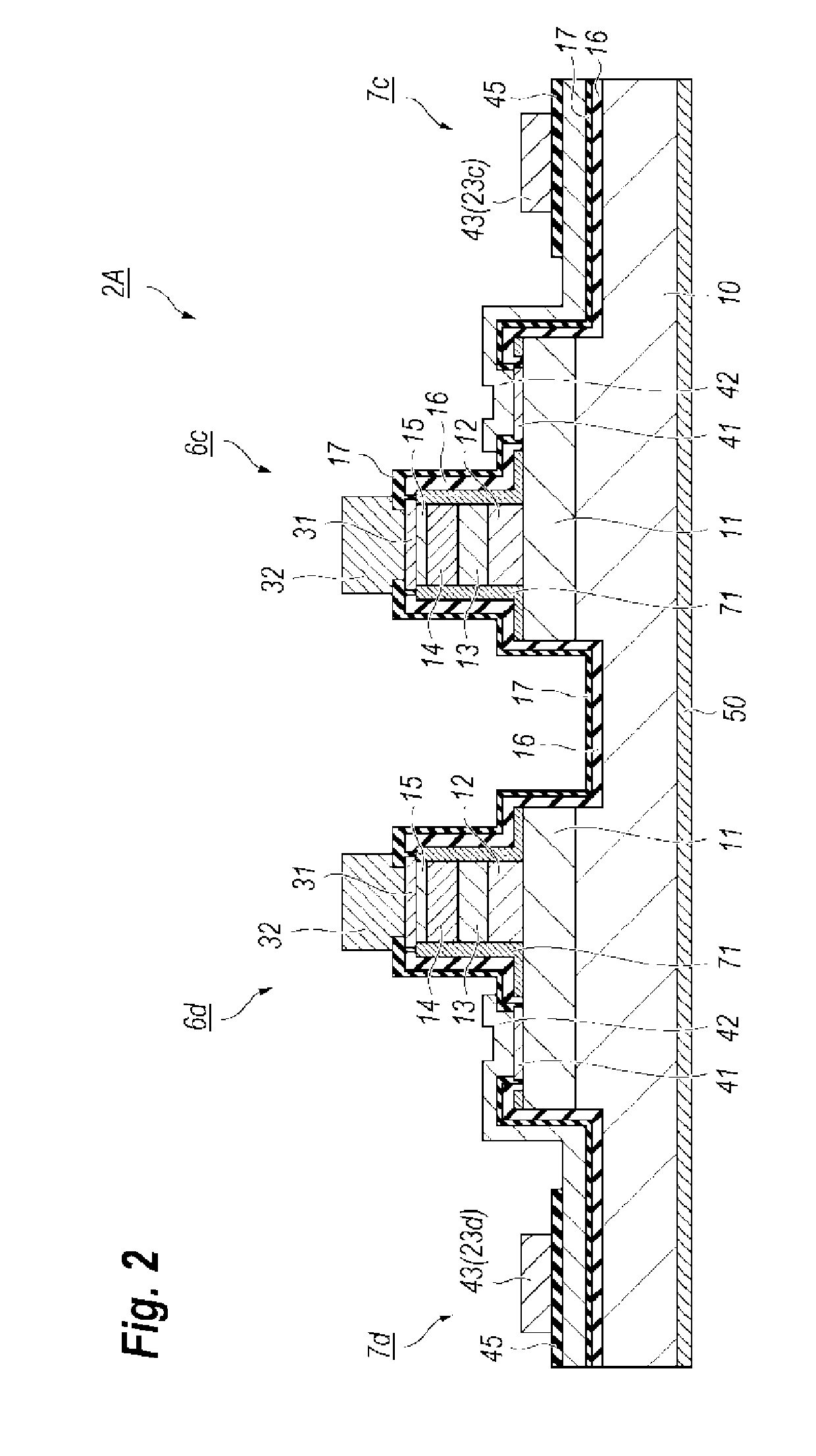
[0072]FIG. 13 is a cross sectional view of another PD device 2C also modified from that shown in FIG. 4, where the cross section shown in FIG. 13 is taken along the line IV-IV indicated in FIG. 1. The PD device 2C has a feature of further implementing the intermediate layer 18 without omitting the buffer layer 12. Other arrangements of the PD device 2C are substantially same with those, 2A and 2B, of the aforementioned embodiment.

[0073]In the arrangement of the PD device2C shown in FIG. 13, a depletion layer at a reversed bias expands from the absorption layer 13 to the buffer layer 12 exceeding the intermediate layer 18, which may enable to further thin the absorption layer 13 without increasing the junction capacitance, or parasitic capacitance between the electrodes. A thinned absorption layer 13 may shorten the carrier transporting time within the absorption layer 13, which may enhance the response of the PD elements, 6a to 6d, in higher frequencies. The present modificatio...


PUM


Abstract

A photodiode (PD) device that monolithically integrates a PD element with a waveguide element is disclosed. The PD device includes a conducting layer with a first region and a second region next to the first region, where the PD element exists in the first region, while, the waveguide element exists in the second region and optically couples with the PD element. The waveguide element includes a core layer and a cladding layer on the conducting layer, which forms an optical confinement structure. The PD element includes an absorption layer on the conducting layer and a p-type cladding layer on the absorption layer, which form another optical confinement structure. The absorption layer has a length at least 12 μm measured from the interface against the core layer.

Description

CROSS REFERENCE TO RELATED APPLICATIONS[0001]The present application claims benefit of Japanese Priority Applications of JP2018-037296 filed on Mar. 2, 2018 and JP2018-090558 filed on May 9, 2018, which are incorporated herein as references.BACKGROUND1. Field of Invention[0002]The present invention relates to a photodiode with a type of optical waveguide.2. Related Background Arts[0003]A Japanese Patent Application laid open No. JP2013-110207A has disclosed a photodiode device that monolithically integrates a waveguide element and a photodiode element with a type of optical waveguide optically coupled with the optical element on a substrate common to the waveguide element and the photodiode element.[0004]An optical communication system currently installed often configures, what is called, the wavelength division multiplexing (WDM) using wavelengths of 1528 to 1565 nm, which is often called as the C-band in the field. As the capacity of data to be transmitted explosively increases, a...

Claims


Application Information

Patent Timeline
Patent Type & Authority Applications(United States)
IPC IPC(8): G02B6/12G02B6/42H01L31/0232H01L31/105H01L31/0304
CPCG02B6/12004G02B6/4206G02B2006/12078H01L31/105H01L31/03042H01L31/02327G02B6/4249H01L31/03046H01L2924/10337
Inventor YONEDA, YOSHIHIROOKIMOTO, TAKUYASAKURAI, KENJI
Owner SUMITOMO ELECTRIC DEVICE INNOVATIONS
Why Eureka
Try Eureka