Silicon based mid-ir super absorber using hyperbolic metamaterial

Inactive Publication Date: 2019-09-26
AMERICAN UNIVERSITY IN CAIRO
View PDF2 Cites 9 Cited by
  • Summary
  • Abstract
  • Description
  • Claims
  • Application Information

AI Technical Summary

Problems solved by technology

Heat losses associated with electronic and electro-optical devices is a major drawback that affects the performance of electronic/photonic circuits.
Unfortunately, broadband absorbers based on coupled resonators results in increase in total thickness of the designed absorber.
Even though these structures

Method used


Image

  • Silicon based mid-ir super absorber using hyperbolic metamaterial
  • Silicon based mid-ir super absorber using hyperbolic metamaterial
  • Silicon based mid-ir super absorber using hyperbolic metamaterial

Examples


Embodiment Construction

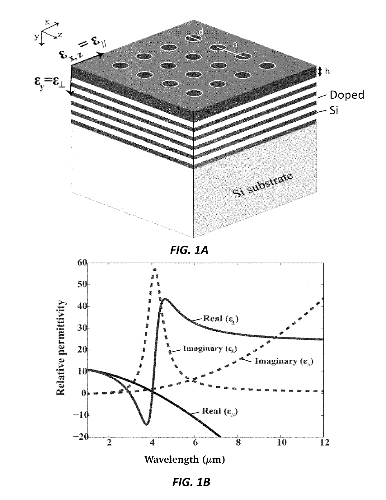
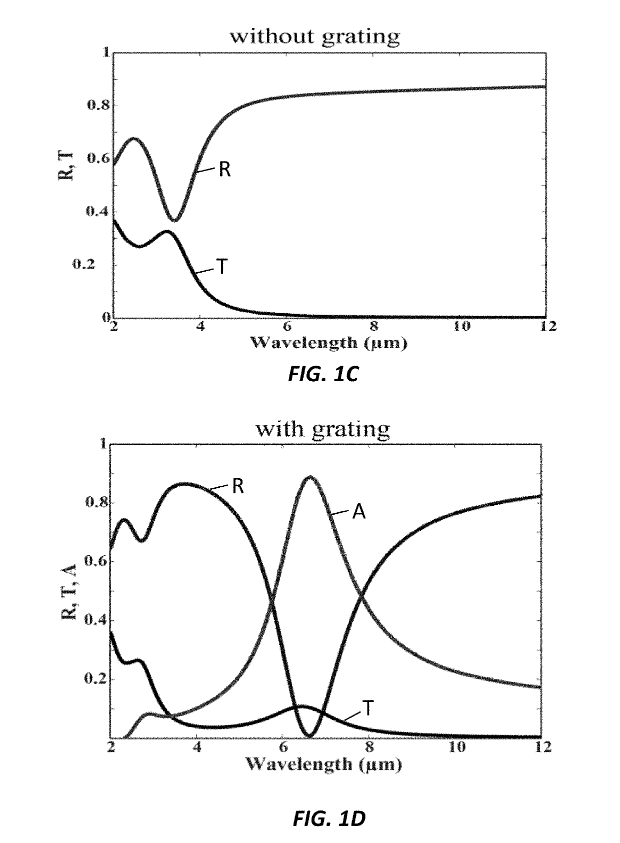
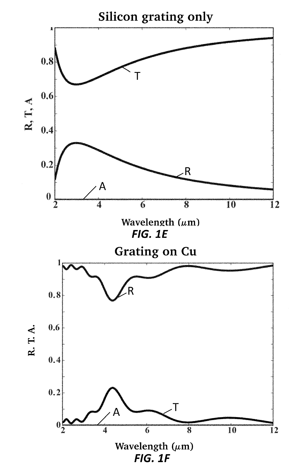
[0019]Perfect absorbers are indispensable components for energy harvesting applications. While many absorbers have been proposed, they encounter inevitable drawbacks including bulkiness or instability over time. The urge for a CMOS compatible absorber that can be integrated for on-chip applications requires further investigation. The current invention demonstrates a Silicon (Si) based mid IR super absorber with absorption (A) reaching 0.948. In one embodiment, the structure is composed of multilayered N-doped Si / Si hyperbolic metamaterial (HMM) integrated with sub-hole Si grating. In another embodiment, the structure has a tunable absorption peak that can be tuned from 4.5 μm to 11 μm through changing the grating parameters. In further embodiments, the invention includes two grating designs integrated with N-doped Si / Si HMM that can achieve wide band absorption. The first grating design is based on Si grating incorporating different holes' height with hole separation distance (a) va...


PUM


Abstract

A broadband hyperbolic metamaterial absorber is provided that includes a substrate layer, a plurality of N-doped silicon layers, a plurality of silicon layers, and a silicon grating layer, where the silicon grating layer includes a pattern of through-holes, where the through-holes have a diameter d, a height h, and a periodic separation distance a, where the plurality of N-doped silicon layers and the plurality of silicon layers are arranged in a stack of alternating layers of N-doped silicon layers and silicon layers disposed on the substrate layer, where the silicon grating layer is disposed on the stack of alternating layers of N-doped silicon layers and silicon layers.

Description

CROSS-REFERENCE TO RELATED APPLICATIONS[0001]This application is a continuation-in-part of U.S. patent application Ser. No. 16 / 244,778 filed Jan. 10, 2019, which is incorporated herein by reference. U.S. patent application Ser. No. 16 / 244,778 filed Jan. 10, 2019 claims benefit of U.S. Provisional Application 62 / 615,690 filed Jan. 10, 2018, which is incorporated herein by reference.FIELD OF THE INVENTION[0002]The present invention relates generally to absorbers for energy harvesting. More particularly, the invention relates to a Silicon (Si) based mid IR super absorber.BACKGROUND OF THE INVENTION[0003]Energy harvesting and handling is an important aspect required for several applications ranging from Microwave range ex: stealth application to near IR ex: thermal photovoltaic. Heat losses associated with electronic and electro-optical devices is a major drawback that affects the performance of electronic / photonic circuits. In order to control the thermal losses in electronic / photonic ...

Claims


Application Information

Patent Timeline
IPC IPC(8): H02S10/30G02B1/00G02B5/18
CPCH02S10/30G02B1/002G02B5/18Y02E10/50B82Y20/00H01L31/02165H01L31/02327
Inventor SWILLAM, MOHAMEDMAHMOUD, AHMED M.DESOUKY, MAI
Owner AMERICAN UNIVERSITY IN CAIRO
Why Eureka
Try Eureka