Method and wafer for fabricating transducer devices

a transducer and wafer technology, applied in piezoelectric/electronic devices, decorative arts, chemical vapor deposition coatings, etc., can solve problems such as wafer warpage, misalignment, and fabrication of transducer/electronic devices, and achieve the effect of reducing or avoiding

Inactive Publication Date: 2019-09-26
CIRRUS LOGIC INT SEMICON
View PDF3 Cites 2 Cited by
  • Summary
  • Abstract
  • Description
  • Claims
  • Application Information

AI Technical Summary

Benefits of technology

[0026]According to the embodiments described herein, there is provided a wafer and a method of f...

Problems solved by technology

In particular, thinning a silicon wafer will make it less rigid and more flexible, which can lead to disadvantages, both to the manufacturing process, and to the transducer/electronic devices being fabricated.
This is particularly problematic when manufacturing MEMS transducer devices such as those described in FIGS. 2a and 2b using wafer level processing, whereby the effect of a reduced wafer thicknesses is enhanced by the manner in which the MEMS transducer devices have an extended cavity 7b defined therein.
This can lead to the wafers becoming warped, or cause sagging during manufacture, i.e. because of the even thinner regions within the MEMS devices being manufactured.
For example, the etched regions in the wafer can lead to less surface area being available for creating a vacuum when a wafer is “held” in place during manufa...

Method used


Image

  • Method and wafer for fabricating transducer devices
  • Method and wafer for fabricating transducer devices
  • Method and wafer for fabricating transducer devices

Examples


Embodiment Construction

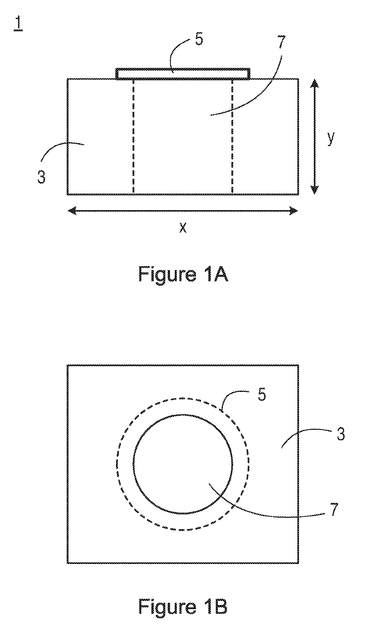
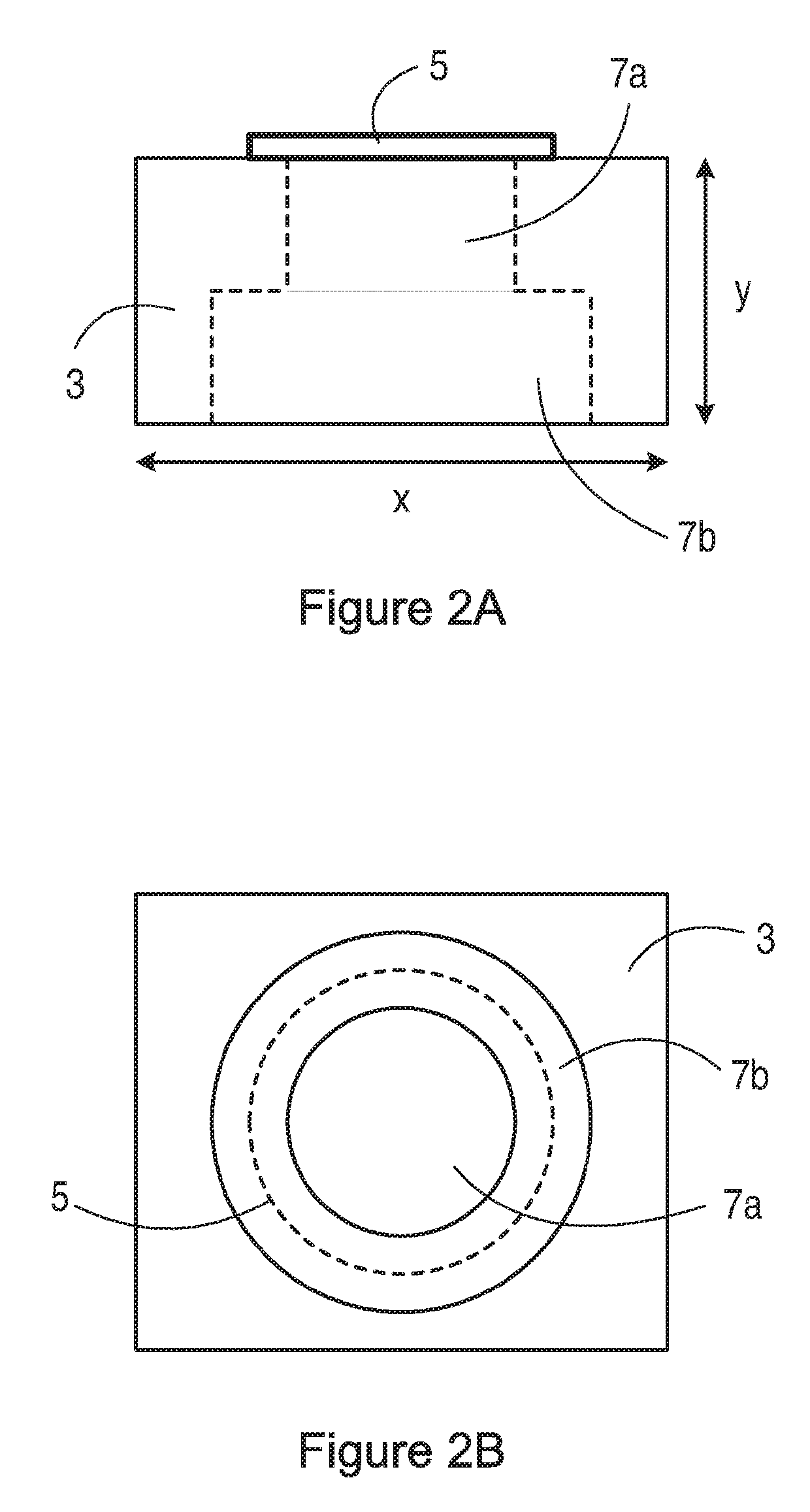
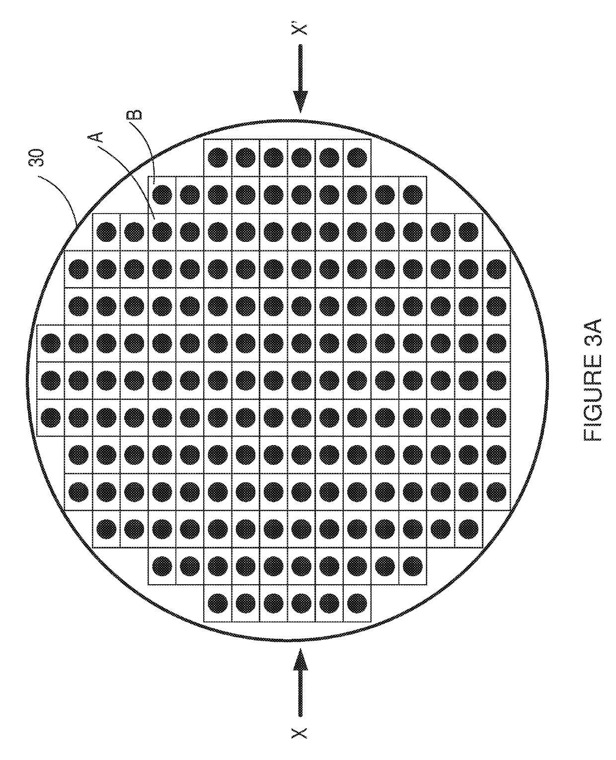
[0052]The embodiments below are described in relation to a wafer, for example a semiconductor wafer such as a silicon wafer, used in the fabrication of transducer devices, for example MEMS transducer devices comprising a substrate and a membrane. It will be appreciated, however, that the invention is equally applicable to fabrication of other forms of transducer or electronic devices, including MEMS transducer devices having different structures, or indeed any other form of device.

[0053]The embodiments described herein are related to a wafer and method of fabrication that reduce wafer process and / or stress variation due to its sag or flexibility. The embodiments herein have an advantage of, on the one hand reducing wafer sag, while on the other not affecting wafer yield significantly i.e. by sacrificing too many MEMS die as a result of allowing space on the wafer for a bracing structure(s).

[0054]As will be described in further detail below, the embodiments herein involve partitionin...


PUM

PropertyMeasurementUnit
Forceaaaaaaaaaa
Molar densityaaaaaaaaaa
Thicknessaaaaaaaaaa

Abstract

A wafer for use in fabricating a plurality of individual transducer devices comprises a bracing structure for partitioning the wafer into a plurality of regions, and a plurality of transducer devices fabricated in one or more of the plurality of regions.

Description

TECHNICAL FIELD[0001]The embodiments described herein relate to a method and wafer for fabricating transducer devices, for example a method and wafer for fabricating transducer devices such as MEMS transducer devices either with or without associated integrated electronics, including for example MEMS capacitive microphones.BACKGROUND OF THE INVENTION[0002]Consumer electronics devices are continually getting smaller and, with advances in technology, are gaining ever-increasing performance and functionality. This is clearly evident in the technology used in consumer electronic products and especially, but not exclusively, portable products such as mobile phones, laptop computers, MP3 players and personal digital assistants (PDAs). Requirements of the mobile phone industry for example, are driving the components to become smaller with higher functionality and reduced cost. It is therefore desirable to integrate functions of electronic circuits together and combine them with transducer ...

Claims


Application Information

Patent Timeline
IPC IPC(8): H04R19/00H04R31/00B81B3/00B81C1/00
CPCB81C1/00658B81B3/007H04R31/00H04R2201/003B81B2201/0257H04R19/005B81B2203/0127B81C1/00666H01L21/78H04R19/04B81B3/00B81C1/00825
Inventor PIECHOCINSKI, MAREK SEBASTIANHOEKSTRA, TSJERK HANS
Owner CIRRUS LOGIC INT SEMICON
Why Eureka
Try Eureka