

Resist composition and patterning process
a composition and composition technology, applied in the field of resist composition and patterning process, can solve the problems of insufficient sensitivity of resist materials described in these patent documents, cdu and lwr to comply with euv lithography, etc., and achieve the effects of high sensitivity, high sensitivity, and high sensitivity
Active Publication Date: 2019-10-24
SHIN ETSU CHEM IND CO LTD
View PDF0 Cites 3 Cited by
- Summary
- Abstract
- Description
- Claims
- Application Information
AI Technical Summary
Benefits of technology
The patent describes a compound that has a high absorption of ultraviolet light and can generate secondary electrons to increase sensitivity. It also has a high atomic weight, which helps prevent acid diffusion and improves the resolution of patterns. This results in a resist composition that has high sensitivity, minimal line width roughness, and improved critical dimension uniformity.
Problems solved by technology
The resist materials described in these patent documents, however, are insufficient in sensitivity, CDU and LWR to comply with the EUV lithography.
Method used
View moreImage
Smart ImageViewing Examples

Examples
example
[0154]Examples and Comparative Examples are given below for further illustrating the invention, but they should not be construed as limiting the invention thereto. All parts (pbw) are by weight.
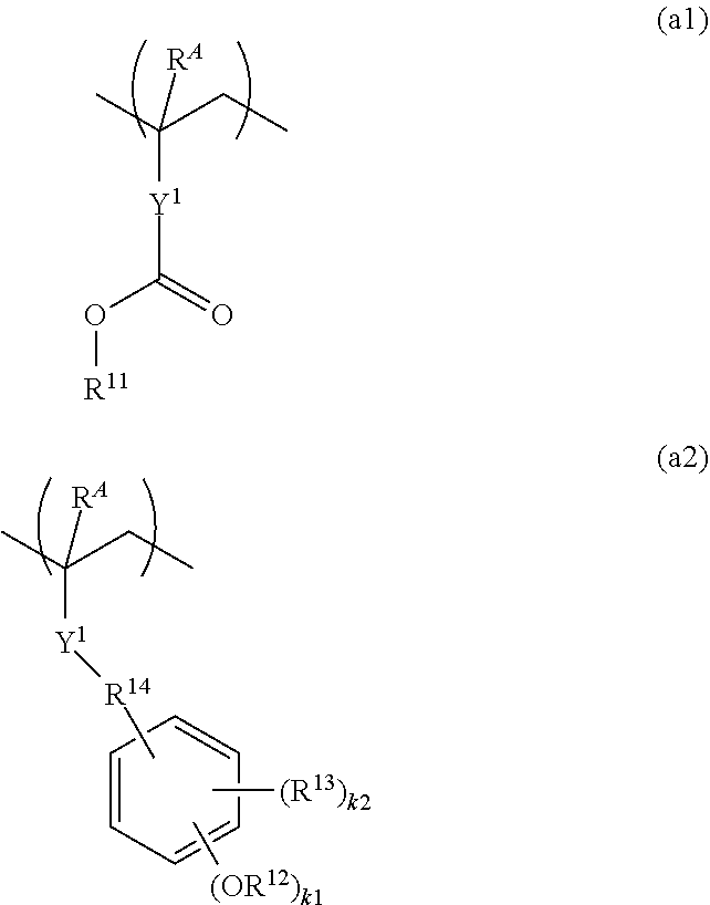
[0155]Sensitizers 1 to 10 used in resist compositions have the structure shown below.
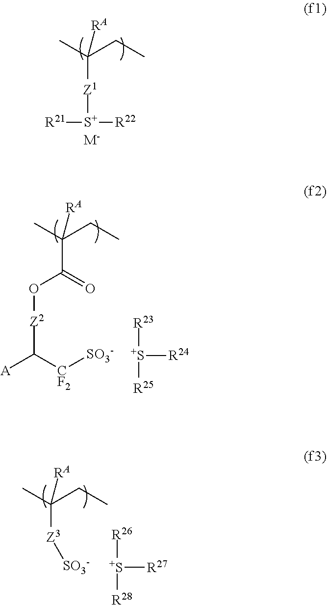
Synthesis Example: Synthesis of Base Polymers, Polymers 1 to 3
[0156]Each of base polymers (Polymers 1 to 3) was prepared by combining monomers in THF solvent, effecting copolymerization reaction, crystallizing from methanol, repeatedly washing with hexane, isolation and drying. The polymer was analyzed for composition by 1H-NMR spectroscopy and for Mw and Mw / Mn by GPC versus polystyrene standards using THF solvent.
Login to View More PUM
| Property | Measurement | Unit |
|---|---|---|
| of wavelength | aaaaa | aaaaa |
| wavelength | aaaaa | aaaaa |
| wavelength | aaaaa | aaaaa |
Abstract
Description
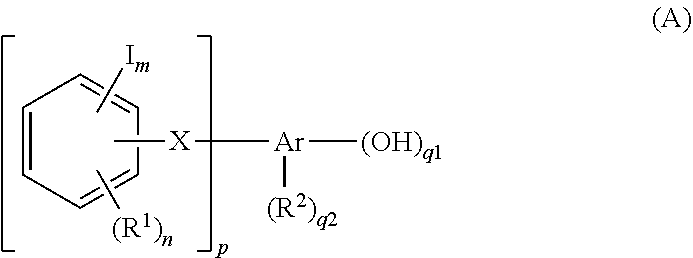
CROSS-REFERENCE TO RELATED APPLICATION[0001]This non-provisional application claims priority under 35 U.S.C. § 119(a) on Patent Application No. 2018-081515 filed in Japan on Apr. 20, 2018, the entire contents of which are hereby incorporated by reference.TECHNICAL FIELD[0002]This invention relates to a resist composition and a patterning process using the composition.BACKGROUND ART[0003]To meet the demand for higher integration density and operating speed of LSIs, the effort to reduce the pattern rule is in rapid progress. The enlargement of the logic memory market in harmony with the wide-spreading of smart phones drives forward the miniaturization technology. As the advanced miniaturization technology, logic devices of 10-nm node are manufactured in a large scale by the double patterning version of ArF immersion lithography. The fabrication of 7-nm node devices of the next generation by the same double patterning process is approaching the mass-scale manufacture stage. EUV lithogr...
Claims
Login to View More Application Information
Patent Timeline
 Patent Type & AuthorityApplications(United States)
IPC IPC(8): G03F7/004G03F7/039G03F7/16G03F7/38G03F7/32G03F7/20
CPCG03F7/0045G03F7/0392G03F7/162G03F7/168G03F7/2004G03F7/322G03F7/2006G03F7/2037G03F7/38G03F7/0397G03F7/0382
InventorHATAKEYAMA, JUNSASAMI, TAKESHI
OwnerSHIN ETSU CHEM IND CO LTD