Cooling of power electronics circuits

a technology for power electronics and circuits, applied in the direction of printed circuit parts, electrical apparatus construction details, printed circuit non-printed electric components association, etc., can solve the problems of not being able to conduct high currents or absorb waste heat, physical large circuit designs, damage or destroy components, etc., to achieve high thermal conductivity and prevent mechanical stresses

Active Publication Date: 2019-10-31
DR ING H C F PORSCHE AG
View PDF11 Cites 4 Cited by
  • Summary
  • Abstract
  • Description
  • Claims
  • Application Information

AI Technical Summary

Benefits of technology

[0027]In one embodiment of the method according to aspects of the invention, to offset slight differences in the physical height between the at least one power electronics component and the at least one metal element, at least one gap pad is positioned at a contact face to the cooling plate....

Problems solved by technology

However, with typical metal thicknesses of 35 μm, such circuit boards, denoted by those skilled in the art as printed circuit boards or PCBs, are not capable of conducting high currents or absorbing the waste heat thereof.
In the background are, in particular, the high parasitic inductances, which result in the case of a physically large circuit design.
Magnetic energy stored in the parasitic inductances can undesirably be discharged in switching processes and generate undesirable switching overvoltages, which damage or destroy components.
However, the etching of copper is substantially isotropically unidirectional and therefore also etches from the side into the copper areas still covered by photoresist.
In the prior art, circuit boards for SMD semiconductors at the surface are provided only with an inlay level and possibly some, usually etched, printed circuit board layers lying above or...

Method used


Image

  • Cooling of power electronics circuits
  • Cooling of power electronics circuits
  • Cooling of power electronics circuits

Examples


Embodiment Construction

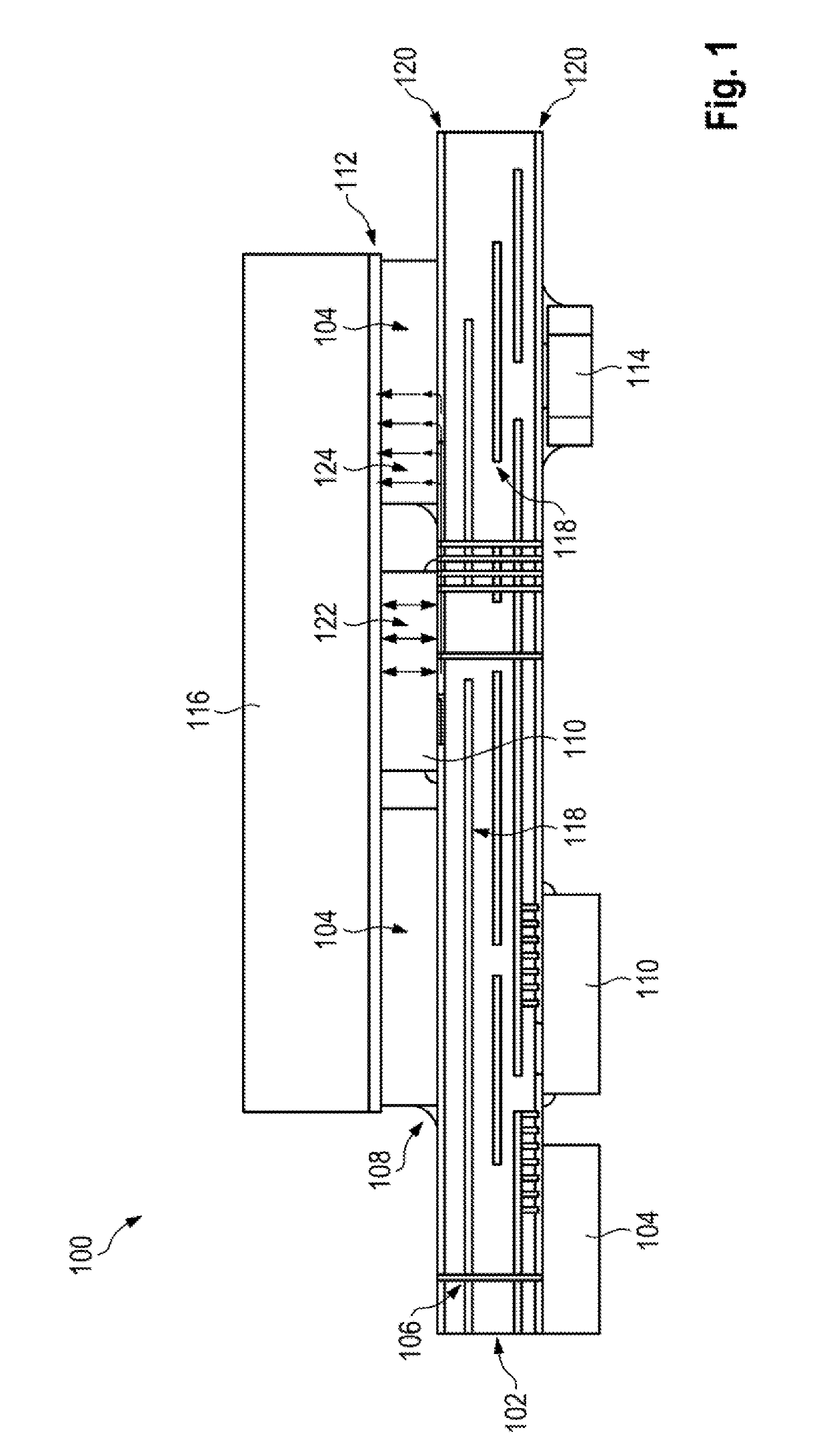
[0049]FIG. 1 shows a schematic illustration 100 of a section through a printed circuit board according to aspects of the invention. A circuit board 102 has inner metallic conductor tracks 118 and, on both surfaces, metallic conductor tracks 120, which run horizontally and can be connected in the vertical direction by means of metallic vias 106. The circuit board 102 is populated on a top side and a bottom side with electronic components, for example shown with a plurality of metal elements 104 and power electronics components 110, and with a capacitor 114 as an example of other components. A respective metal element 104 is situated on a conductor track 120 running on a respective surface of the circuit board 102. Said metal element has a flat top side and has a similar physical height to a respective power electronics component 110. By way of example, said metal element is connected to the circuit board 102 at a location 108 by solder. The power electronics component 110, which may ...


PUM


Abstract

A method for cooling power electronics circuits, in which a printed circuit board is produced according to a prescribed circuit board process and is populated with at least one power electronics components. Contact connecting at least one location on at least one metallic conductor track running on a surface of the printed circuit board that includes at least one metal element, which is both electrically conductive and heat-conductive and the physical height of which is designed to be at least as large as that of the at least one power electronics component. A cooling plate is placed in a planar manner onto the at least one power electronics component and/or the at least one metal element.

Description

CROSS-REFERENCE TO RELATED APPLICATION[0001]This application claims priority to German Patent application No. DE 10 2018 109 920.7, filed Apr. 25, 2018, which is incorporated by reference herein in its entirety.FIELD OF THE INVENTION[0002]The present invention relates to a method for cooling power electronics circuits, in which at least one conductor track on a printed circuit board is designed with respect to possibilities for dissipating heat. A printed circuit board designed in such a way is also described herein.BACKGROUND OF THE INVENTION[0003]Conventional power electronics systems are usually implemented with discrete electrical components, for example thyristors and IGBTs, shortened by those skilled in the art for insulated-gate bipolar transistors, with screw connections and busbars. In contrast, recent power transistors permit integration of high-power circuits into typical circuit boards. However, with typical metal thicknesses of 35 μm, such circuit boards, denoted by tho...

Claims


Application Information

Patent Timeline
IPC IPC(8): H05K1/02H05K1/18H05K7/20
CPCH05K1/181H05K2201/10522H05K2201/064H05K2201/10015H05K1/0204H05K7/20927H05K1/0203H05K1/18H05K7/20509H05K1/0209H05K7/205H05K7/209H05K2201/066H05K2201/10166H01L23/3735H05K1/0207H05K7/20254
Inventor GÖTZ, STEFANSPECHT, EDUARD
Owner DR ING H C F PORSCHE AG
Why Eureka
Try Eureka