Display device
a technology of display device and display screen, which is applied in the direction of identification means, semiconductor devices, instruments, etc., can solve the problems of large energy loss, constant energy consumption of light source, and waste of light in either case, and achieves high yield, low defect rate, and high manufacturing yield.
- Summary
- Abstract
- Description
- Claims
- Application Information
AI Technical Summary
Benefits of technology
Problems solved by technology
Method used
Image

Examples
first embodiment
[0101]Hereinafter, an embodiment of the present invention will be described in detail with reference to FIG. 1 to FIG. 25.
(Configuration of LED Display Chip)
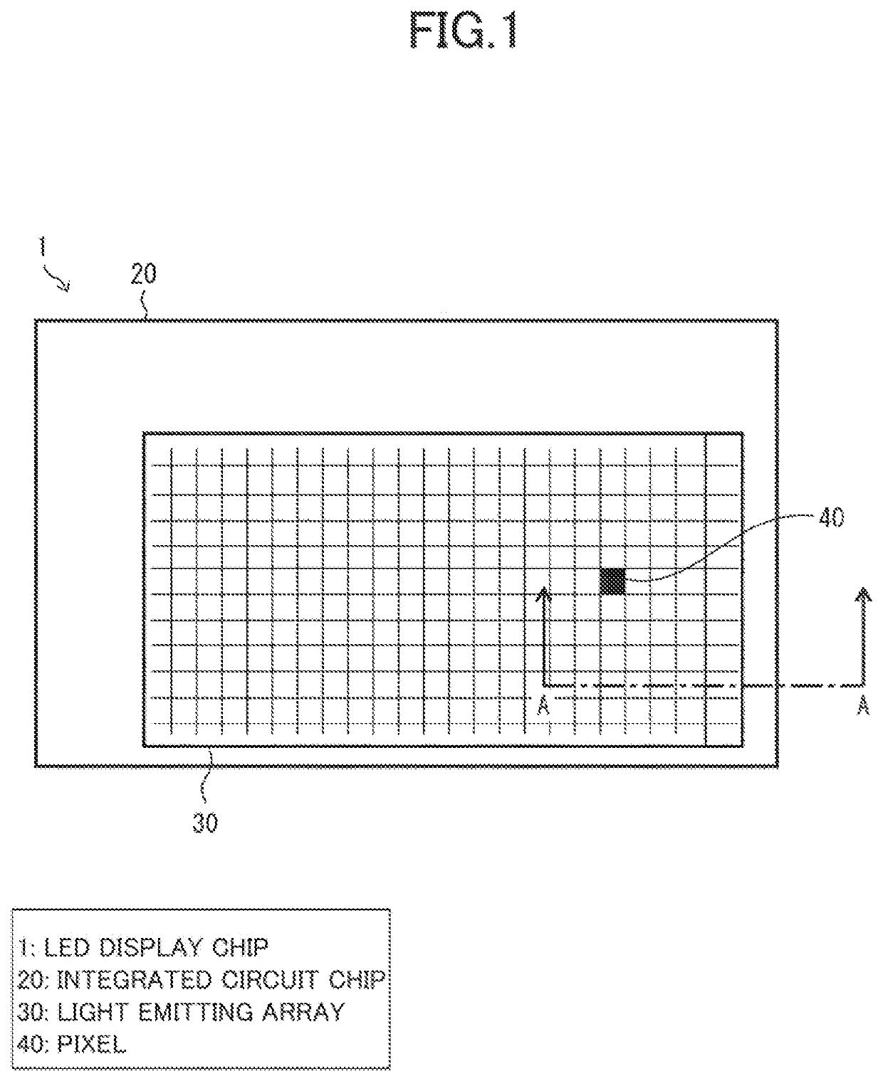
[0102]Hereinafter, a schematic configuration of an LED display chip 1 will be described.
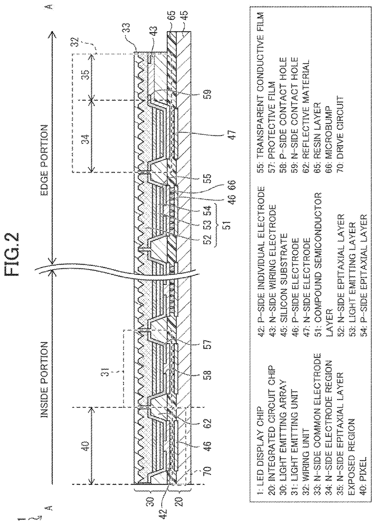
[0103]FIG. 1 is a schematic diagram for describing the schematic configuration of the LED display chip 1 according to a first embodiment of the present invention. FIG. 1 is a top view of the LED display chip 1.
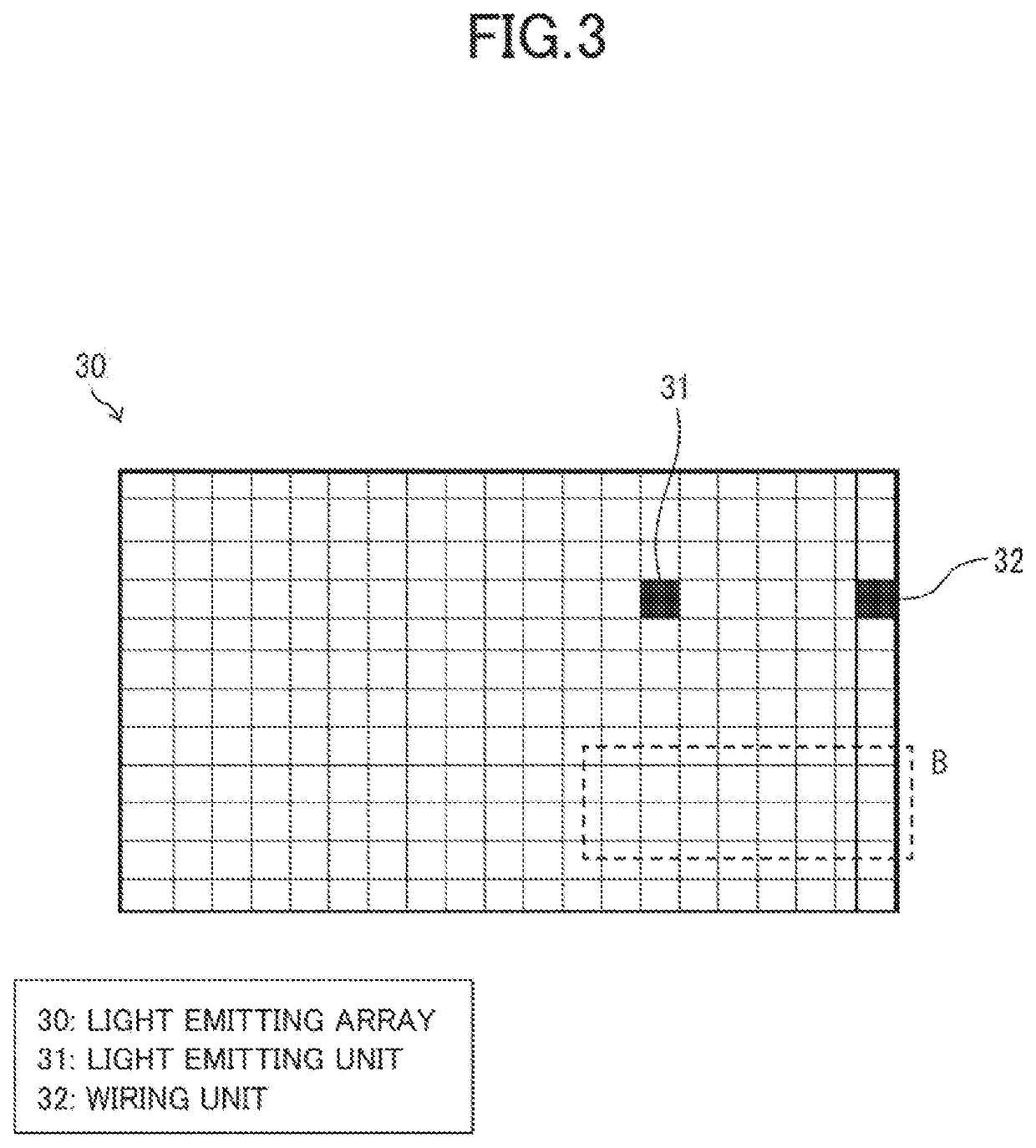
[0104]As illustrated in FIG. 1, the LED display chip 1 includes an integrated circuit (IC) chip 20 and a light emitting array 30 mounted on a mounting surface of the IC chip 20 (integrated circuit device). The LED display chip 1 may arbitrarily include an adhesive layer (not illustrated) including a resin layer, metallic particles, or the like for bonding the IC chip 20 and the light emitting array 30, a wavelength conversion layer (not illustrated) for converting the wavelength of light emitted by the light emitting array 30, and so fo...
first modification example
[0191]Hereinafter, a detailed description will be given of a modification example of manufacturing steps of manufacturing the LED display chip 1 in the case of providing a wavelength conversion layer 68 in the LED display chip 1, with reference to FIG. 21 to FIG. 23. FIG. 21 to FIG. 23 illustrate an exemplary sequence of manufacturing steps subsequent to the steps illustrated in FIG. 16 to FIG. 19 in order. Thus, reference numerals in a figure illustrating a preceding step will appropriately be omitted in a figure illustrating a subsequent step for the sake of simplicity.
[0192]FIG. 21 to FIG. 23 are diagrams illustrating exemplary steps that are per after the steps illustrated in FIG. 16 to FIG. 19 in the case of providing the wavelength conversion layer 68.
[0193]Subsequently to the step illustrated in FIG. 19, a difference in level between the IC chip 20 and the light emitting array 30 is reduced by using a planarizing layer 67, as illustrated in FIG. 21. The planarizing layer 67 i...
second modification example
[0201]Hereinafter, a detailed description will be given of a modification example of manufacturing steps of manufacturing the LED display chip 1 in the case of moving the light emitting array 30 onto a peel substrate 63 and a transfer substrate 64, with reference to FIG. 24. Parts (a) to (e) of FIG. 24 illustrate an exemplary sequence of manufacturing steps subsequent to the steps illustrated in FIG. 9 to FIG. 15 in order. Thus, reference numerals in a figure illustrating a preceding step will appropriately be omitted in a figure illustrating a subsequent step for the sake of simplicity.
[0202]FIG. 24 is a diagram illustrating exemplary steps that are performed subsequently to the steps illustrated in FIG. 9 to FIG. 15 in the case of moving the light emitting array 30 onto the peel substrate 63 and the transfer substrate 64.
[0203]The method for mounting the light emitting array 30 on the IC chip 20 may be a method for moving the light emitting array 30 onto the peel substrate 63 and ...
PUM
 Abstract
Description
Claims
Application Information
 - Generate Ideas
- Intellectual Property
- Life Sciences
- Materials
- Tech Scout
- Unparalleled Data Quality
- Higher Quality Content
- 60% Fewer Hallucinations
Browse by: Latest US Patents, China's latest patents, Technical Efficacy Thesaurus, Application Domain, Technology Topic, Popular Technical Reports.
© 2025 PatSnap. All rights reserved.Legal|Privacy policy|Modern Slavery Act Transparency Statement|Sitemap|About US| Contact US: help@patsnap.com