Semiconductor memory device
- Summary
- Abstract
- Description
- Claims
- Application Information
AI Technical Summary
Benefits of technology
Problems solved by technology
Method used
Image


Examples
first embodiment
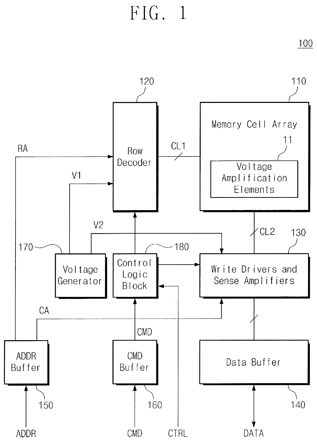
[0041]FIG. 3 shows a memory cell MC according to a The memory cell MC connected to the first conductive line CL1_1, the 2a-th conductive line CL2a_1, and the 2b-th conductive line CL2b_1 is illustrated in FIG. 3.
[0042]The memory cell MC may include first to sixth transistors T1 to T6. The first transistor T1 and the second transistor T2 may be serially connected between a power node to which a power supply voltage VDD is supplied and a ground node to which a ground voltage VSS is supplied. The first transistor T1 may be a PMOS transistor, and the second transistor T2 may be an NMOS transistor.
[0043]The third transistor T3 and the fourth transistor T4 may be serially connected between the power node to which the power supply voltage VDD is supplied and the ground node to which the ground voltage VSS is supplied. The third transistor T3 may be a PMOS transistor, and the fourth transistor T4 may be an NMOS transistor.
[0044]The fifth transistor T5 may be connected between gates of the ...
second embodiment
[0057]FIG. 5 illustrates a memory cell MC according to a The memory cell MC connected to the first conductive line CL1_1, the 2a-th conductive line CL2a 1, and the 2b-th conductive line CL2b_1 is illustrated in FIG. 5.
[0058]The memory cell MC may include a selection element SE and a variable resistance element RE functioning as a storage element. The selection element SE may include a transistor connected between the variable resistance element RE and the 2a-th conductive line CL2a_1 and is controlled by a voltage of the first conductive line CL1_1.
[0059]The variable resistance element RE may be connected between the selection element SE and the 2b-th conductive line CL2b_1. The variable resistance element RE may have a resistance value that varies with a voltage applied to the variable resistance element RE or a current flowing through the variable resistance element RE. Data may be stored in the variable resistance element RE by adjusting a resistance value of the variable resist...
third embodiment
[0063]FIG. 6 illustrates a memory cell MC according to a The memory cell MC connected to the first conductive line CL1_1, the 2a-th conductive line CL2a_1, and the 2b-th conductive line CL2b_1 is illustrated in FIG. 6.
[0064]The memory cell MC may include the selection element SE and a capacitor “C” functioning as a storage element. The selection element SE may include a transistor connected between the capacitor “C” and the 2a-th conductive line CL2a_1 and is controlled by a voltage of the first conductive line CL1_1. The capacitor “C” may store data by charging or discharging a voltage. The memory cell MC may be a dynamic random access memory (DRAM) cell.
[0065]A transistor of the selection element SE may be implemented identically to the transistor described with reference to FIG. 4. For example, a gate insulating layer of the transistor of the selection element SE may include a ferroelectric material. The transistor of the selection element SE may be implemented to include the vo...
PUM
 Abstract
Description
Claims
Application Information
 - R&D
- Intellectual Property
- Life Sciences
- Materials
- Tech Scout
- Unparalleled Data Quality
- Higher Quality Content
- 60% Fewer Hallucinations
Browse by: Latest US Patents, China's latest patents, Technical Efficacy Thesaurus, Application Domain, Technology Topic, Popular Technical Reports.
© 2025 PatSnap. All rights reserved.Legal|Privacy policy|Modern Slavery Act Transparency Statement|Sitemap|About US| Contact US: help@patsnap.com