
Charge pump circuit and phase-locked loop

a charge pump and phase lock technology, applied in the field of integrated circuits, can solve the problems of increasing the complexity of the circuit, bringing certain hidden dangers to the overall stability of the circuit, and increasing the design difficulty of the operational amplifier, and achieve the effect of simple circuit structur

Active Publication Date: 2020-02-13
CHINA COMM MICROELECTRONICS TECH CO LTD +1
View PDF0 Cites 2 Cited by
  • Summary
  • Abstract
  • Description
  • Claims
  • Application Information

AI Technical Summary

Benefits of technology

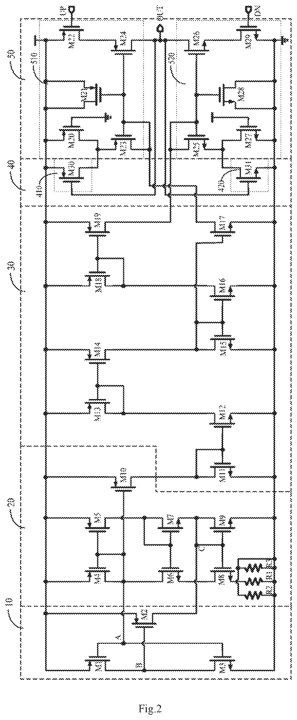
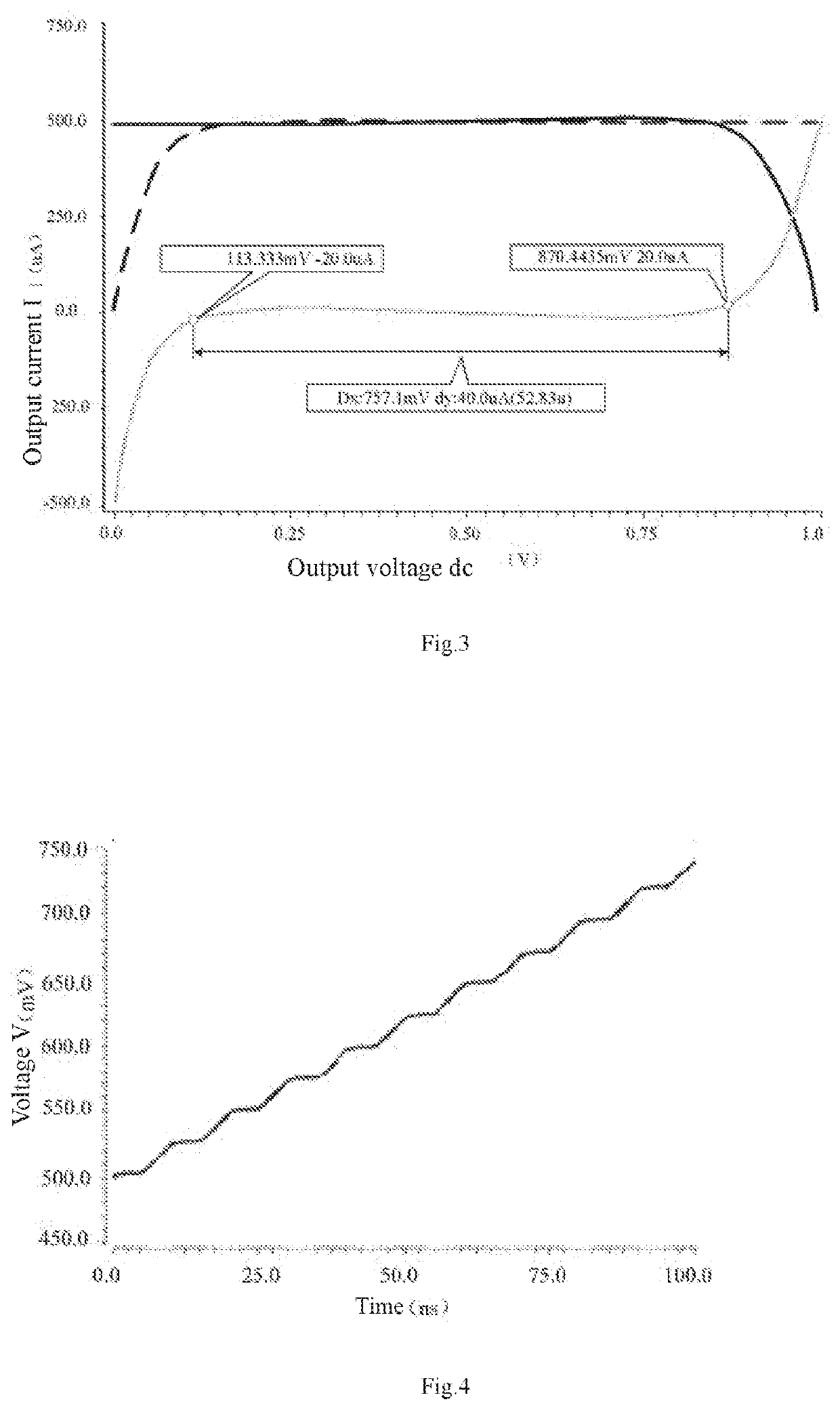
The patent describes a charge pump circuit and a phase-locked loop that can match the charging and discharging currents of a charge pump without needing an extra operational amplifier. This is achieved by using a charging and discharging feedback control module that detects the output voltage of the charge pump and controls the charging and discharging currents accordingly to prevent any mismatches between them. This results in a wide output voltage range where the charging and discharging currents match. The charge pump circuit has a simple structure and is suitable for low-voltage working environments.

Problems solved by technology

In a traditional circuit structure realizing the match of the charging current and the discharging current of a charge pump circuit, an operational amplifier circuit is used to hold the voltage between different nodes, which not only increases the complexity of the circuit, but also brings certain hidden dangers to the overall stability of the circuit.
Meanwhile, in order to realize a large output voltage swing, the structure of an operational amplifier needs to realize rail-to-rail input and output characteristics, which further increases the design difficulty of the operational amplifier.
Moreover, an operational amplifier working at low voltages often has low operating frequencies and cannot be applied to high-frequency fields.

Method used


Image

  • Charge pump circuit and phase-locked loop
  • Charge pump circuit and phase-locked loop
  • Charge pump circuit and phase-locked loop

Examples


Embodiment Construction

[0027]In order to facilitate the understanding of the present invention, the present invention will be described more fully below with reference to the relevant drawings. Preferred embodiments of the present invention are shown in the accompanying drawings. However, the present invention may be implemented in many different ways and is not limited to the embodiments described herein. On the contrary, the purpose of providing these embodiments is to make the understanding to the disclosure of the present invention more thorough and comprehensive.

[0028]Unless otherwise defined, all technical and scientific terms used herein have the same meaning as commonly understood by those skilled in the technical field of the present invention. The terms used herein in the description of the present invention are for the purpose of describing specific embodiments only and are not intended to limit the present invention. As used herein, the term “and / or” includes any and all combinations of one or...


PUM


Abstract

A charge pump circuit and phase-locked loop include start, bias, current mirror, charging and discharging feedback control, and charging and discharging matching modules, which are electrically connected in sequence. The start module starts the bias module. The bias module generates constant bias current and outputs same to the current mirror module, which receives and amplifies the bias current for output in two paths. The charging and discharging feedback control module detects the output voltage of a charge pump and controls, according to feedback of the output voltage, the current in the charging and discharging matching module, to suppress the mismatch between charging and discharging currents. The charging and discharging matching module receives an external charging or discharging control signal, to charge or discharge the output load of the charge pump. Charging and discharging currents can be matched within a wide output voltage range, without an operational amplifier.

Description

BACKGROUND OF THE INVENTION1. Technical Field[0001]The invention relates to the technical field of integrated circuits, in particular to a low-voltage and wide-output range charge pump circuit and a phase-locked loop.2. Description of Related Art[0002]As one of the most popular frequency synthesizer structures in modern wireless communication system applications, a phase locked loop (PLL) can realize signal modulation and demodulation, as well as clock recovery, and generate local oscillator signals for carrier recovery of a mixer and a wireless receiver. A charge pump phase-locked loop (CP-PLL) has become the most common phase-locked loop circuit due to the characteristics of high speed and low noise. A charge pump (CP) circuit plays a very important role in a charge pump phase-locked loop. The main function of the charge pump circuit is to convert UP and DN pulse digital signals from a phase frequency detector (PFD) into analog voltage signals through a low-pass filter (LPF), and ...

Claims


Application Information

Patent Timeline
Patent Type & Authority Applications(United States)
IPC IPC(8): H03L7/089H02M3/07
CPCH03L7/0895H02M3/07H03L7/0891H02M1/36H03L7/0896
Inventor DING, QINGZHOU, HAIFENGWU, GUANGSHENGLI, XIAOCONG
Owner CHINA COMM MICROELECTRONICS TECH CO LTD
Learn More