Nitride semiconductor device and method for manufacturing same

Active Publication Date: 2020-04-02
PANASONIC INTELLECTUAL PROPERTY MANAGEMENT CO LTD
View PDF0 Cites 14 Cited by
  • Summary
  • Abstract
  • Description
  • Claims
  • Application Information

AI Technical Summary

Benefits of technology

[0013]The semiconductor device according to the present disclosure can easily realize normally-OFF operation and can simultaneously realize a low ON resistance even without forming a recess part immediately under the third nitride semiconductor layer, which therefore permits realization of simple processes at low costs.
[0014]Moreover, presence of the fourth nitride semiconductor layer makes it possi

Problems solved by technology

However, the semiconductor device described in International Publication WO2014/174810 faces a following problem.
However, thinning even the second nitride semiconductor layer located immediately under the drain electrode part in a similar manner depletes even an area immediately under the drain electrode part, which deteriorates the ON resistance.
However, providing the

Method used


Image

  • Nitride semiconductor device and method for manufacturing same
  • Nitride semiconductor device and method for manufacturing same
  • Nitride semiconductor device and method for manufacturing same

Examples


embodiment

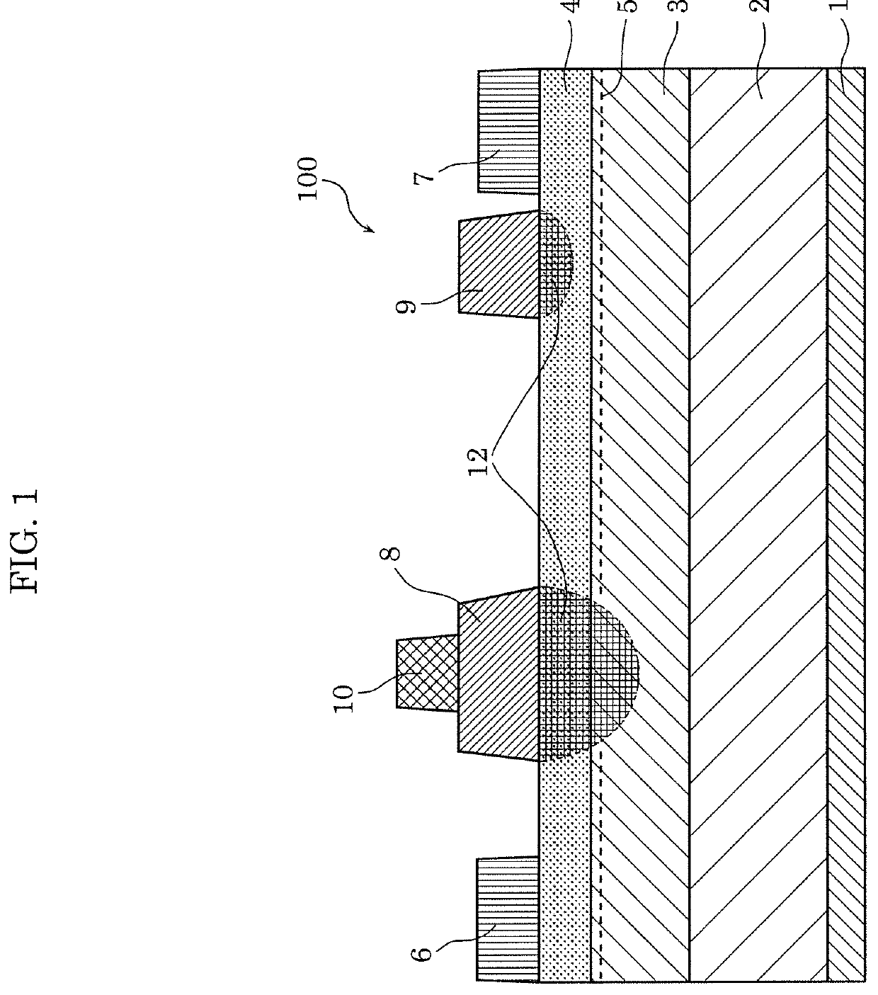
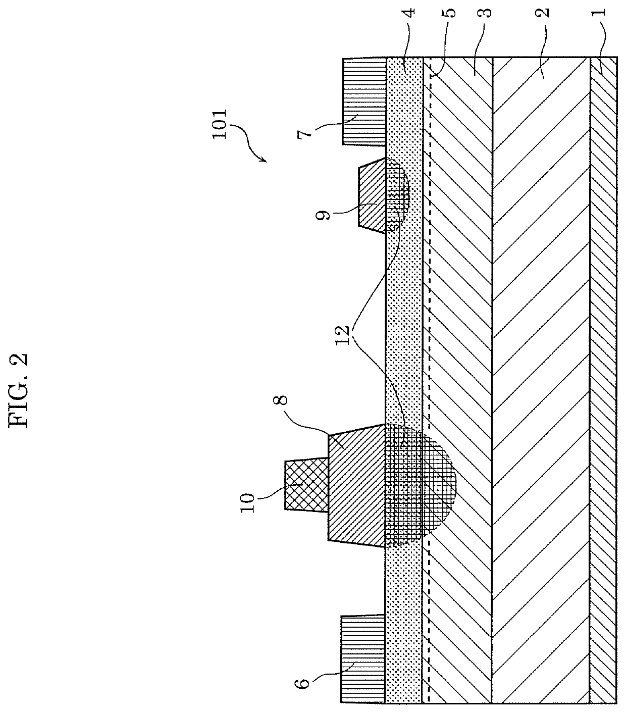
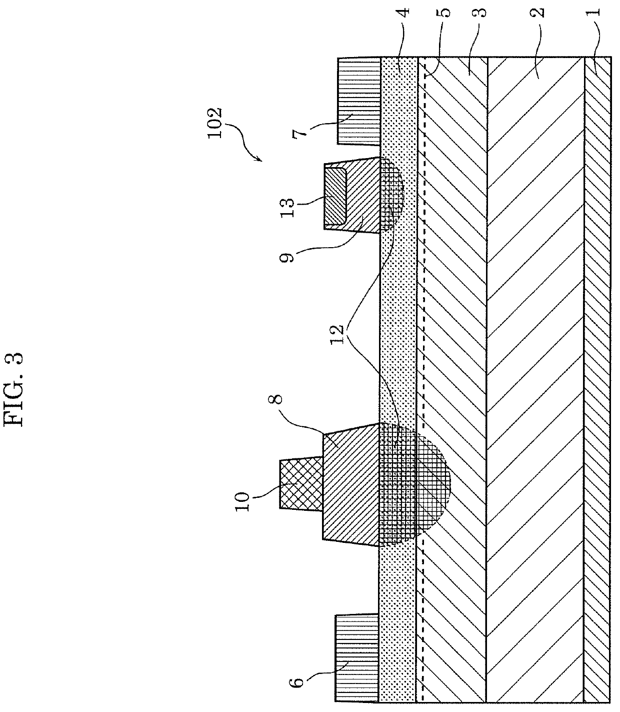
[0027]FIG. 1 illustrates a sectional structure of the nitride semiconductor device according to the embodiment. Nitride semiconductor device 100 according to Embodiment 1 is characterized by having: third nitride semiconductor layer 8 containing a p-type first impurity and serving as a gate; and fourth nitride semiconductor layer 9, between a third nitride semiconductor layer 8 region and drain electrode 7, containing a p-type second impurity. The nitride semiconductor device according to the embodiment is also characterized in that the average carrier concentration of the fourth nitride semiconductor layer is lower than the average carrier concentration of the third nitride semiconductor layer.

[0028]Nitride semiconductor device 100 has, on appropriate Si substrate 1 (alternatively, for example, Sapphire, SiC, GaN, or AlN substrate), appropriate buffer layer 2 (for example, a signal layer or multiple layers of, for example, GaN, AlGaN, AlN, InGaN, or AlInGaN as a group-III nitride s...


PUM


Abstract

A nitride semiconductor device includes: a substrate; a first nitride semiconductor layer; a second nitride semiconductor layer having a greater band gap than the first nitride semiconductor layer; a source electrode and a drain electrode on the second nitride semiconductor layer apart from each other; a third nitride semiconductor layer, between the source electrode and the drain electrode, containing a p-type first impurity and serving as a gate; and a fourth nitride semiconductor layer, between the third nitride semiconductor layer and the drain electrode, containing a p-type second impurity, wherein the average carrier concentration of the fourth nitride semiconductor layer is lower than the average carrier concentration of the third nitride semiconductor layer.

Description

CROSS REFERENCE TO RELATED APPLICATION[0001]This application claims the benefit of priority of Japanese Patent Application Number 2018-182424 filed on Sep. 27, 2018, the entire content of which is hereby incorporated by reference.BACKGROUND1. Technical Field[0002]The present disclosure relates to a structure of a semiconductor device and a method for manufacturing the semiconductor device, and more specifically to a device using a semiconductor, a group-III nitride semiconductor in particular, which can be used as, for example, a power transistor and a method for manufacturing the device.2. Description of the Related Art[0003]A group-III nitride semiconductor has a wide band gap and thus a high dielectric breakdown voltage. The group-III nitride semiconductor can also easily form a heterostructure of, for example, AlGaN and GaN, can generate an electron channel (two-dimensional electron gas 2 DEG) with high mobility and a high concentration on a GaN layer side of an AlGaN / GaN interf...

Claims


Application Information

Patent Timeline
IPC IPC(8): H01L29/778H01L29/20H01L29/205H01L29/417H01L29/36H01L29/207H01L29/66H01L21/02H01L29/43
CPCH01L21/0262H01L29/66462H01L21/0274H01L21/02381H01L29/2003H01L21/2233H01L21/2236H01L29/7787H01L21/30621H01L29/36H01L29/205H01L21/0254H01L29/207H01L29/41758H01L29/432H01L29/0619H01L29/32H01L29/41725H01L29/7786H01L29/1066
Inventor OKITA, HIDEYUKIYANAGIHARA, MANABUSATO, TAKAHIROHIKITA, MASAHIRO
Owner PANASONIC INTELLECTUAL PROPERTY MANAGEMENT CO LTD
Why Eureka
Try Eureka