Three-dimensional image sensor, optical radar apparatus, and processing apparatus

a technology of optical radar and image sensor, applied in the field of three-dimensional image sensor, can solve the problems of weak comparison of laser light intensity on an object, increase in cost and an increase in the size of the apparatus, and reduce the accuracy of distance measurement, so as to achieve the effect of wide measurement rang

Active Publication Date: 2020-04-30
SHARP KK
View PDF0 Cites 9 Cited by
  • Summary
  • Abstract
  • Description
  • Claims
  • Application Information

AI Technical Summary

Benefits of technology

[0016]In an aspect of the present invention, it is possible to realize a low-cost three-dimensional image sensor capable of providing a wide measurement range.

Problems solved by technology

The scan-based irradiation techniques require a mechanical mechanism for scanning the beam, which results in an increase in cost and an increase in an apparatus size.
But the laser light intensity on an object is weak compared to the scan-based irradiation technique.
Therefore, when the distance to the object is large, the signal strength is low, which results in a reduction in the distance measurement accuracy.

Method used


Image

  • Three-dimensional image sensor, optical radar apparatus, and processing apparatus
  • Three-dimensional image sensor, optical radar apparatus, and processing apparatus
  • Three-dimensional image sensor, optical radar apparatus, and processing apparatus

Examples


embodiment 1

[0029]Embodiment 1 of the present invention is described below with reference to FIGS. 1 to 9.

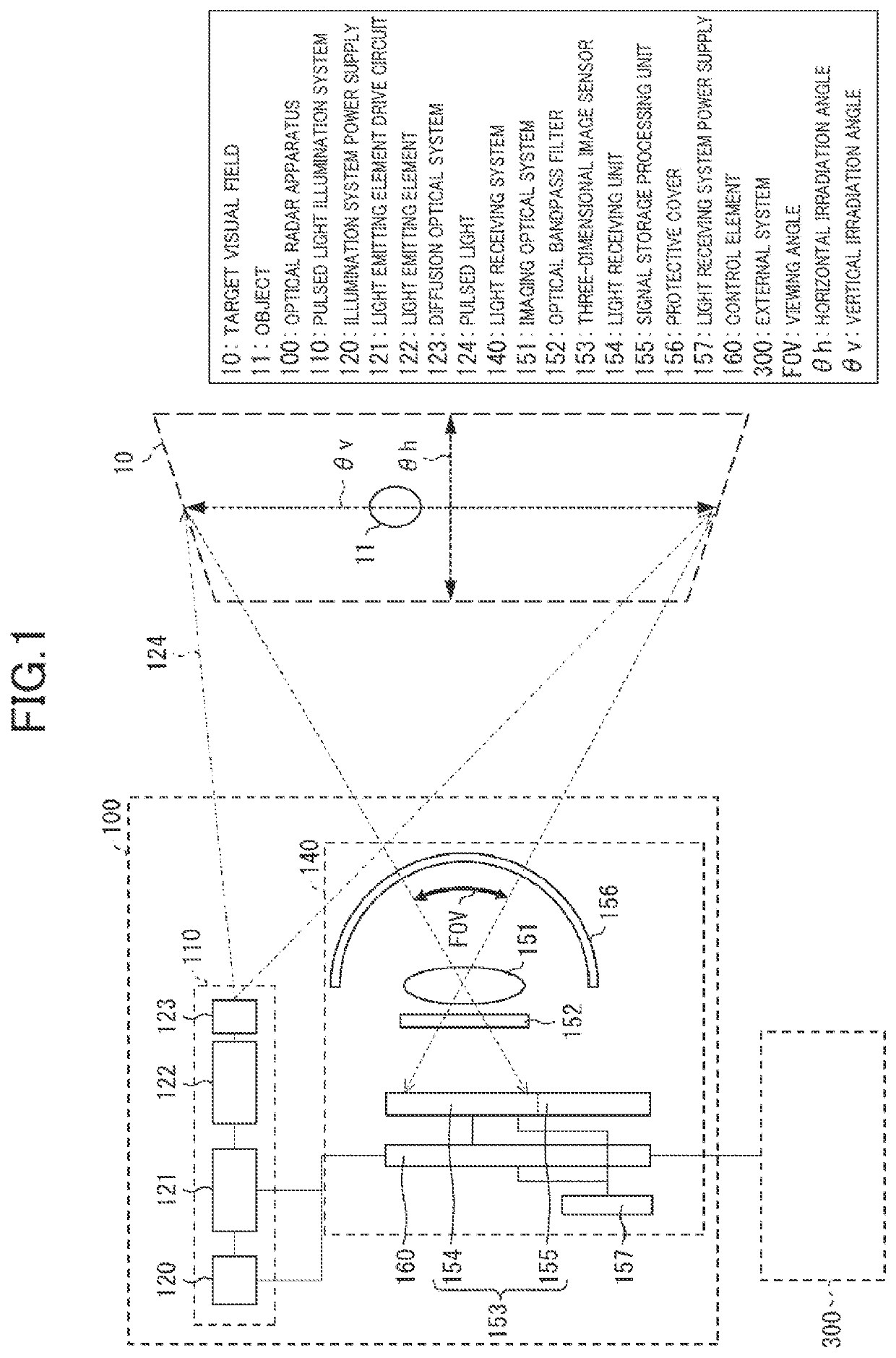
[0030]FIG. 1 is a schematic diagram showing a configuration of an optical radar apparatus 100 according to the present embodiment

100>

[0031]As shown in FIG. 1, the optical radar apparatus 100 includes a pulsed light illumination system 110 configured to irradiate a target visual field 10 with pulsed light 124, and a light receiving system 140 configured to receive light from at least a part of the target visual field 10.

[0032]The pulsed light illumination system 110 includes an illumination system power supply 120, a light emitting element drive circuit 121, a diffusion optical system 123, and a light emitting element 122. The diffusion optical system 123 simultaneously irradiates the entire target visual field 10 with the pulsed light 124 emitted from the light emitting element 122. The light emitting element drive circuit 121 is a circuit configured to perform pulse-driving on the light em...

embodiment 2

[0137]Embodiment 2 of the present invention is described below with reference to FIG. 10.

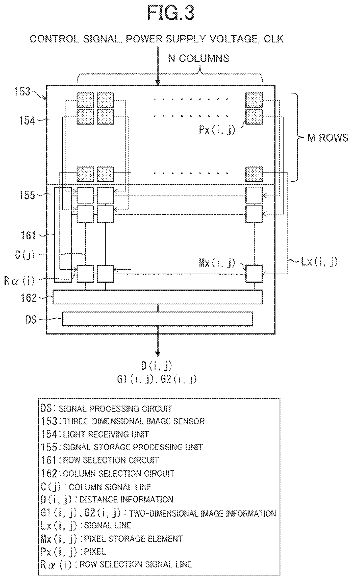
[0138]FIG. 10 is a flow chart illustrating a signal processing procedure by the signal processing circuit DS in the three-dimensional image sensor 153 of the optical radar apparatus 100 according to the present embodiment.

[0139]The optical radar apparatus 100 according to the present embodiment is the same as that of the first embodiment except that the distance extraction algorithm used by the signal processing circuit DS is different from that of the first embodiment. The distance extraction algorithm according to the first embodiment is simple, but a measurement error tends to often occur when the difference between the number of counts NCβ(t) and the number of counts NC1(t) is small, or when the difference between NC(β+1)(t) and NC1(t) is small. The algorithm described below improves the situation described above. FIG. 10 is a schematic diagram illustrating a signal processing procedure by t...

embodiment 3

[0154]Embodiment 3 of the present invention is described below with reference to FIG. 11.

[0155]FIG. 11 is a block diagram showing a configuration of the three-dimensional image sensor 153 constituting the optical radar apparatus 100 according to the present embodiment.

[0156]The essential difference of the present embodiment from Embodiment 1. Is that the maximum number of binary counters BCα constituting the pixel storage element Mx(i,j) is increased to 21. In order to improve the distance measurement accuracy, the full width at half maximum ΔT of the pulsed light was reduced to ΔT=10 nsec so as to be 1 / 10 of that in Embodiment 1. The distance estimation algorithm used is Embodiment 1 is also employed in the present embodiment. The details will be described below.

[0157]By setting ΔT=ΔTα=10 nsec (α>1), it is possible to improve the time resolution. However, the number of binary counters BCα is increased to 21, which causes an increase in the area of the pixel storage elements Mx(i,j)...


PUM


Abstract

An object is to realize a low-cost three-dimensional image sensor capable of providing a wide measurement range. The three-dimensional image sensor includes a light receiving unit including a plurality of pixels each including an SPAD (single-photon avalanche photodiode) configured to detect, in Geiger mode, a photon of incident light including reflected light from an object to be detected, a plurality of pixel storage elements provided for the respective pixels in a one-to-one manner, each pixel storage unit being configured to count a accumulated value of pulse signals output from a corresponding one of the pixels as a result of detecting photons for each of temporally successive time intervals, and a signal processing circuit (DS) configured to calculate distance information regarding a distance between a light receiving unit and an object for each pixel by using groups of accumulated values accumulated by the pixel storage elements.

Description

TECHNICAL FIELD[0001]The present invention relates to a three-dimensional image sensor configured to acquire a three-dimensional image including a two-dimensional image of an object and distance information regarding a distance to the object.BACKGROUND ART[0002]A three-dimensional image is a concept that includes distance information regarding a distance to an object in a field of view in addition to a two-dimensional image such as a usual photograph. In recent years, a three-dimensional image sensor for detecting such a three-dimensional image has become extremely important as a sensor used for recognition of an environment around a vehicle, a robot, and the like. CCD and CMOS imagers are widely used as two-dimensional image sensors for detecting two-dimensional images. Both CCD and CMOS imagers convert light intensity into electric signals using silicon photodiodes thereby obtaining images. In a widely used method of measuring a distance with high accuracy, a target object is irra...

Claims


Application Information

Patent Timeline
Patent Type & Authority Applications(United States)
IPC IPC(8): H04N13/254G01S17/894G01S7/4863G01S7/4865
CPCH01L27/14643H01L27/14623H01L27/14627H04N13/254G01S7/4863G01S17/894G01C3/06H04N13/271G01S7/4865G01S7/487
Inventor IGUCHI, KATSUJI
Owner SHARP KK
Why Eureka
Try Eureka