Logic drive based on chip scale package comprising standardized commodity programmable logic IC chip and memory IC chip

a logic drive and chip scale technology, applied in the direction of power consumption reduction, pulse technique, instruments, etc., can solve the problems of higher fabrication cost, lower fabrication yield, and more power consumption, and achieve flexible, programmable and powerful functions and operations.

Active Publication Date: 2020-05-21
ICOMETRUE CO LTD
View PDF0 Cites 23 Cited by
  • Summary
  • Abstract
  • Description
  • Claims
  • Application Information

AI Technical Summary

Benefits of technology

[0034]The processing and / or computing IC chip or chips in the logic drive provide fixed-metal-line (non-field-programmable) interconnects for (non-field-programmable) functions, processors and operations. The standard commodity FPGA IC chips provide (1) programmable-metal-line (field-programmable) interconnects for (field-programmable) logic functions, processors and operations and (2) fixed-metal-line (non-field-programmable) interconnects for (non-field-programmable) logic functions, processors and operations. Once the programmable-metal-line interconnects in or of the FPGA IC chips are programmed, the programmed interconnects together with the fixed interconnects in or of the FPGA chips provide some specific functions for some given applications. The operational FPGA chips may operate together with the processing and / or computing IC chip or chips in the same logic drive to provide flexibility, programmability and powerful functions and operations in applications, for example, Artificial Intelligence (AI), machine learning, deep learning, big data, Internet Of Things (IOT), industry computing, Virtual Reality (VR), Augmented Reality (AR), driverless car electronics, Graphic Processing (GP), Digital Signal Processing (DSP), Micro Controlling (MC), and / or Central Processing (CP).

Problems solved by technology

The switch from the FPGA design to the ASIC or COT design is because the current FPGA IC chip, for a given application and compared with an ASIC or COT chip, (1) has a larger semiconductor chip size, lower fabrication yield, and higher fabrication cost, (2) consumes more power, (3) gives lower performance.
The high NRE cost in implementing the innovation or application using the advanced IC technology nodes or generations slows down or even stops the innovation or application using advanced and useful semiconductor technology nodes or generations.

Method used


Image

  • Logic drive based on chip scale package comprising standardized commodity programmable logic IC chip and memory IC chip
  • Logic drive based on chip scale package comprising standardized commodity programmable logic IC chip and memory IC chip
  • Logic drive based on chip scale package comprising standardized commodity programmable logic IC chip and memory IC chip

Examples


Embodiment Construction

[0184]Illustrative embodiments are now described. Other embodiments may be used in addition or instead. Details that may be apparent or unnecessary may be omitted to save space or for a more effective presentation. Conversely, some embodiments may be practiced without all of the details that are disclosed.

[0185]Specification for Static Random-Access Memory (SRAM) Cells

[0186](1) First Type of Volatile Storage Unit

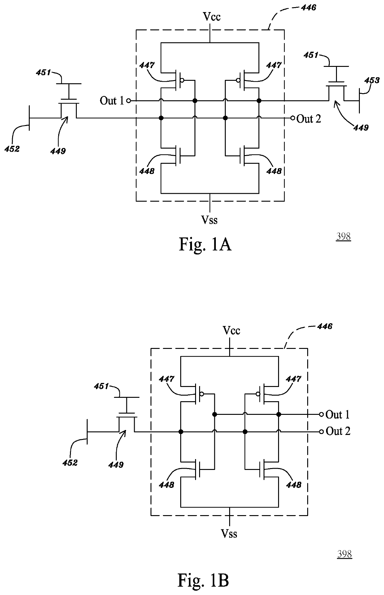
[0187]FIG. 1A is a circuit diagram illustrating a first type of volatile storage unit in accordance with an embodiment of the present application. Referring to FIG. 1A, a first type of volatile storage unit 398 may have a memory unit 446, i.e., static random-access memory (SRAM) cell, composed of 4 data-latch transistors 447 and 448, that is, two pairs of a P-type MOS transistor 447 and N-type MOS transistor 448 both having respective drain terminals coupled to each other, respective gate terminals coupled to each other and respective source terminals coupled to the voltage ...


PUM


Abstract

A multi-chip package includes: a first semiconductor integrated-circuit (IC) chip; a second semiconductor integrated-circuit (IC) chip over and bonded to the first semiconductor integrated-circuit (IC) chip; a plurality of first metal posts over and coupling to the first semiconductor integrated-circuit (IC) chip, wherein the plurality of first metal posts are in a space beyond and extending from a sidewall of the second semiconductor integrated-circuit (IC) chip; and a first polymer layer over the first semiconductor integrated-circuit (IC) chip and in the space, wherein the plurality of first metal posts are in the first polymer layer, wherein a top surface of the first polymer layer, a top surface of the second semiconductor integrated-circuit (IC) chip and a top surface of each of the plurality of first metal posts are coplanar.

Description

PRIORITY CLAIM[0001]This application claims priority benefits from U.S. provisional application No. 62 / 768,978, filed on Nov. 18, 2018 and entitled “LOGIC DRIVE BASED ON STANDARDIZED COMMODITY PROGRAMMABLE LOGIC / MEMORY SEMICONDUCTOR IC CHIP SCALE PACKAGES”, U.S. provisional application No. 62 / 882,941, filed on Aug. 5, 2019 and entitled “VERTICAL INTERCONNECT ELEVATOR BASED ON THROUGH SILICON VIAS”, and U.S. provisional application No. 62 / 891,386, filed on Aug. 25, 2019 and entitled “VERTICAL INTERCONNECT ELEVATOR BASED ON THROUGH SILICON VIAS”. The present application incorporates the foregoing disclosures herein by reference.BACKGROUND OF THE DISCLOSUREField of the Disclosure[0002]The present invention relates to a logic package, logic package drive, logic device, logic module, logic drive, logic disk, logic disk drive, logic solid-state disk, logic solid-state drive, Field Programmable Gate Array (FPGA) logic disk, FPGA logic drive, or programmable logic drive (to be abbreviated a...

Claims


Application Information

Patent Timeline
Patent Type & Authority Applications(United States)
IPC IPC(8): H01L23/538H01L25/065G11C5/06H03K19/094
CPCH01L25/0657G11C5/06H01L23/5386H01L23/5385H01L23/5384H03K19/094H01L2224/0401H01L25/18H01L2225/06513H01L2225/06541H01L25/0652H01L25/50H01L25/03H01L2224/73259H01L2924/18161H01L2224/73204H01L2224/92125H01L2224/32145H01L2224/08145H01L2224/04105H01L2224/12105H01L2224/94H01L2924/18162H01L2225/1035H01L2225/1058H01L2225/1094H01L25/105H01L2225/1041H01L2224/97H01L2924/15192H01L2224/81005H01L2224/83005H01L2224/92224H01L25/0655H01L2924/15311H01L24/19H01L23/5389H01L23/5383H01L23/49816H01L21/76898H01L23/481H01L23/49811H01L24/05H01L24/08H01L24/13H01L24/16H01L24/80H01L24/81H01L2224/05547H01L2224/05571H01L2224/06181H01L2224/13022H01L2224/13025H01L2224/13082H01L2224/14181H01L2224/16146H01L2224/16235H01L2224/16238H01L2224/17181H01L2224/32225H01L2224/33181H01L2224/80011H01L2224/80013H01L2224/80097H01L2224/8083H01L2224/80895H01L2224/80896H01L2224/81191H01L2224/81193H03K19/1737H03K3/356113H03K3/012H03K19/0013H03K19/0016H03K19/018521H03K19/018592H03K19/177H01L2224/05647H01L2224/13109H01L2224/05186H01L2224/13144H01L2224/13111H01L2224/05166H01L2224/05147H01L2224/05686H01L2224/13139H01L2224/05666H01L2224/2919H01L2224/13147H01L2224/81H01L2224/83H01L2224/80001H01L2224/16225H01L2924/00H01L2224/16145H01L2924/00014H01L2924/0665H01L2924/014H01L2924/0105H01L2924/01079H01L2924/04941H01L2924/01029H01L2924/01047H01L2924/01049
Inventor LIN, MOU-SHIUNGLEE, JIN-YUAN
Owner ICOMETRUE CO LTD
Why Eureka
Try Eureka