A method of additive manufacture of a waveguide as well as waveguide devices manufactured according to this method

Active Publication Date: 2020-05-21
SWISSTO 12 SA
View PDF0 Cites 5 Cited by
  • Summary
  • Abstract
  • Description
  • Claims
  • Application Information

AI Technical Summary

Benefits of technology

[0031]The hole or holes allow a more even conductive metal deposition by preventing the accumulation of bubbles in the channel, and allowing improved fluid exchange between the inside and the outside of the waveguide during deposition.
[0032]The holes are particularly useful for preventing reagent stagnation ne

Problems solved by technology

Manufacturing waveguides with complex sections is difficult and expensive.
However, the problem is complex because of the small size of the opening, the complex shapes that it is often necessary to cover, and the need to control with great precision the dimensions of the opening and therefore the thickness of the coating.
The deposition of this intermediate layer is difficult; in this publication, it is in the form of a conductive ink of about 50 microns.
The electrical connection of the portions of the cathode that are difficult to reach within the waveguide is also problematic.
First, the frequent presence of trapped air bubbles in the waveguide channel often causes insufficient plating, or even a complete lack of plating, on some surfaces. The a

Method used


Image

  • A method of additive manufacture of a waveguide as well as waveguide devices manufactured according to this method
  • A method of additive manufacture of a waveguide as well as waveguide devices manufactured according to this method
  • A method of additive manufacture of a waveguide as well as waveguide devices manufactured according to this method

Examples


Example

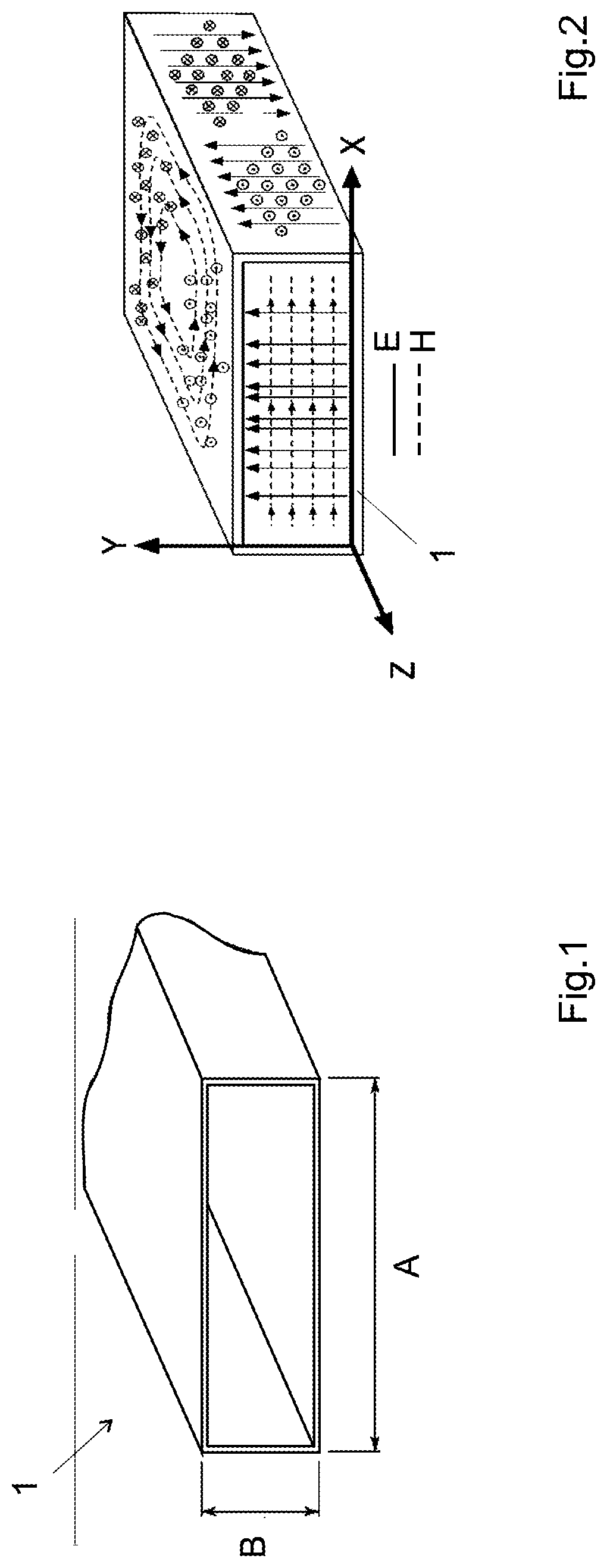
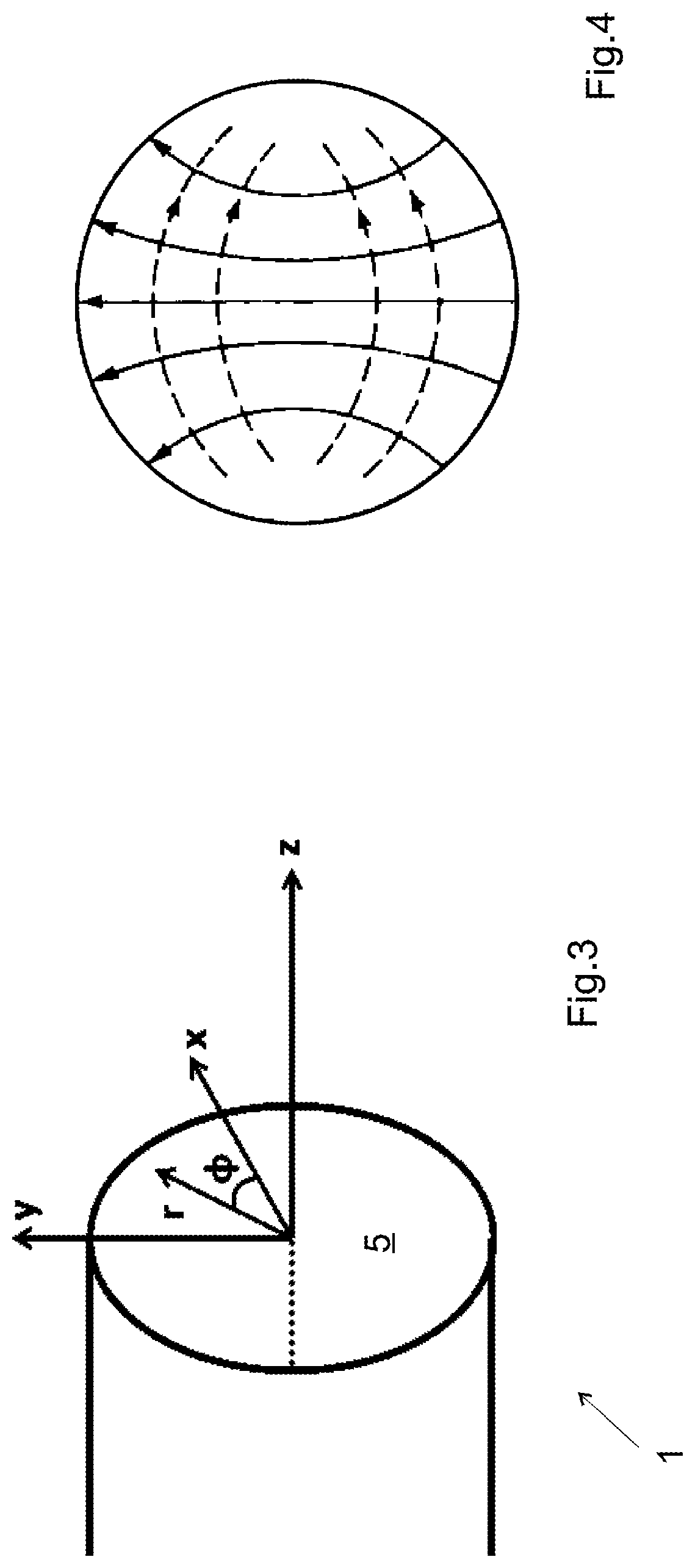
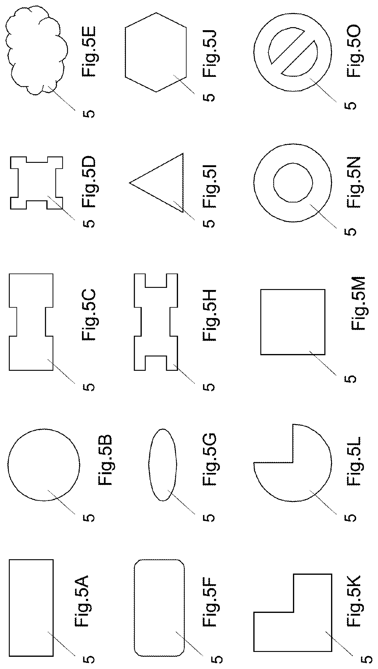
[0067]FIG. 7 illustrates a perspective view of a waveguide device 1 according to the invention, in this case a waveguide device having a rectangular section. It comprises a core 2 of non-conductive material, for example of polymer such as epoxy, or ceramic, manufactured by additive manufacturing, for example by stereolithography. This core delimits an internal channel 5 designed for waveguiding, and whose section is determined according to the frequency of the electromagnetic signal to transmit. The dimensions of this internal channel a, b and its shape are determined as a function of the operating frequency of the device 1, i.e. the frequency of the electromagnetic signal for which the device is manufactured and for which a transmission mode that is stable and optionally has a minimum of attenuation is obtained.

[0068]The core 5 is made monolithically, for example by stereolithography. It may also consist of several parts formed by stereolithography and assembled together before pla...


PUM

PropertyMeasurementUnit
Lengthaaaaaaaaaa
Diameteraaaaaaaaaa
Lengthaaaaaaaaaa

Abstract

A method for producing a waveguide device, including producing a core of a non-conductive material. The core has side walls with outer surfaces and inner surfaces, the inner surfaces defining a waveguide channel. A layer of conductive metal is deposited on the inner surfaces by immersion in a fluid of reactants. The core includes at least one hole between the outer and inner surfaces, specifically used to encourage the removal of bubbles from the channel and/or the circulation of the fluid during the immersion.

Description

TECHNICAL FIELD[0001]The present invention relates to a method for the additive manufacturing of a waveguide device and a waveguide manufactured according to this method.STATE OF THE ART[0002]Radio Frequency (RF) signals can propagate either in a space or in waveguide devices. These waveguide devices are used to channel the RF signals or to manipulate them in the spatial or frequency domain.[0003]The present invention relates in particular to passive RF devices that make it possible to propagate and manipulate radio frequency signals without the use of active electronic components. Passive waveguides can be divided into three distinct categories:[0004]Devices based on waveguiding inside hollow metal channels, commonly called waveguides.[0005]Devices based on waveguiding inside dielectric substrates.[0006]Devices based on waveguiding by means of surface waves on metal substrates such as PCB (printed circuit boards), microstrips, etc.[0007]The present invention relates in particular t...

Claims


Application Information

Patent Timeline
IPC IPC(8): H01P11/00H01P3/123B33Y80/00B33Y10/00
CPCH01P11/002B33Y10/00B33Y80/00H01P3/123H01Q21/064H01P3/12Y10T29/49016
Inventor DE RIJK, EMILEFAVRE, MIRKOBILLOD, MATHIEUDIMITRIADES, ALEXANDREMACOR, ALESSANDRO
Owner SWISSTO 12 SA
Why Eureka
Try Eureka