Circuit structure and method of manufacturing the same

a technology of circuit structure and manufacturing method, which is applied in the direction of semiconductor devices, semiconductor/solid-state device details, electrical apparatus, etc., can solve the problems of increasing manufacturing costs, increasing manufacturing costs, and increasing the cost of manufacturing, so as to prevent adhesion and imc problems, improve the structural strength of the conductive layer and the conductive bump in the circuit structure, and improve product reliability.

Inactive Publication Date: 2020-08-06
WINBOND ELECTRONICS CORP
View PDF0 Cites 1 Cited by
  • Summary
  • Abstract
  • Description
  • Claims
  • Application Information

AI Technical Summary

Benefits of technology

[0007]In view of the above, the 3D printing technology is applied in the disclosure to form the circuit layer (including the conductive layer and the conductive bump), so that the conductive layer and the conductive bump are integrally formed. Namely, the conductive layer and the conductive bump are made of the same material in the same manufacturing step, so as to prevent the adhesion and IMC issues between differen...

Problems solved by technology

In addition to the cumbersome steps, the yield loss, material waste, and diversification of the manufacturing machine in the plural manufacturing processes lead to the increase in the manufacturing costs.
Besides, the adhesion issue may occur in layers of the multi...

Method used


Image

  • Circuit structure and method of manufacturing the same
  • Circuit structure and method of manufacturing the same
  • Circuit structure and method of manufacturing the same

Examples


Embodiment Construction

[0012]The invention will be described in a more comprehensive manner with reference to the drawings of the embodiments. This invention, however, may be embodied in many different forms and should not be construed as limited to the embodiments set forth herein. The thickness of layers and regions in the drawings may be exaggerated for clarity. The same or similar reference numbers used in the embodiments represent the same or similar devices. Accordingly, no further description thereof is provided hereinafter.

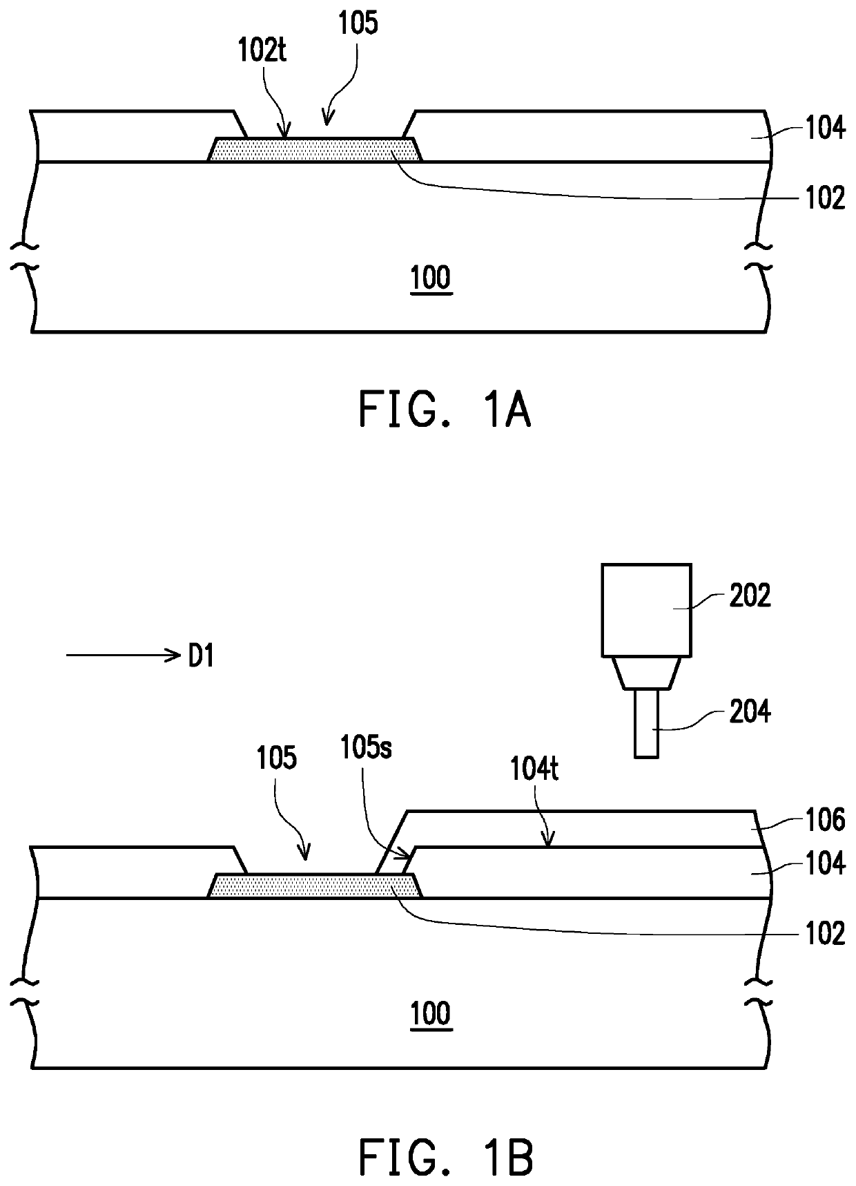
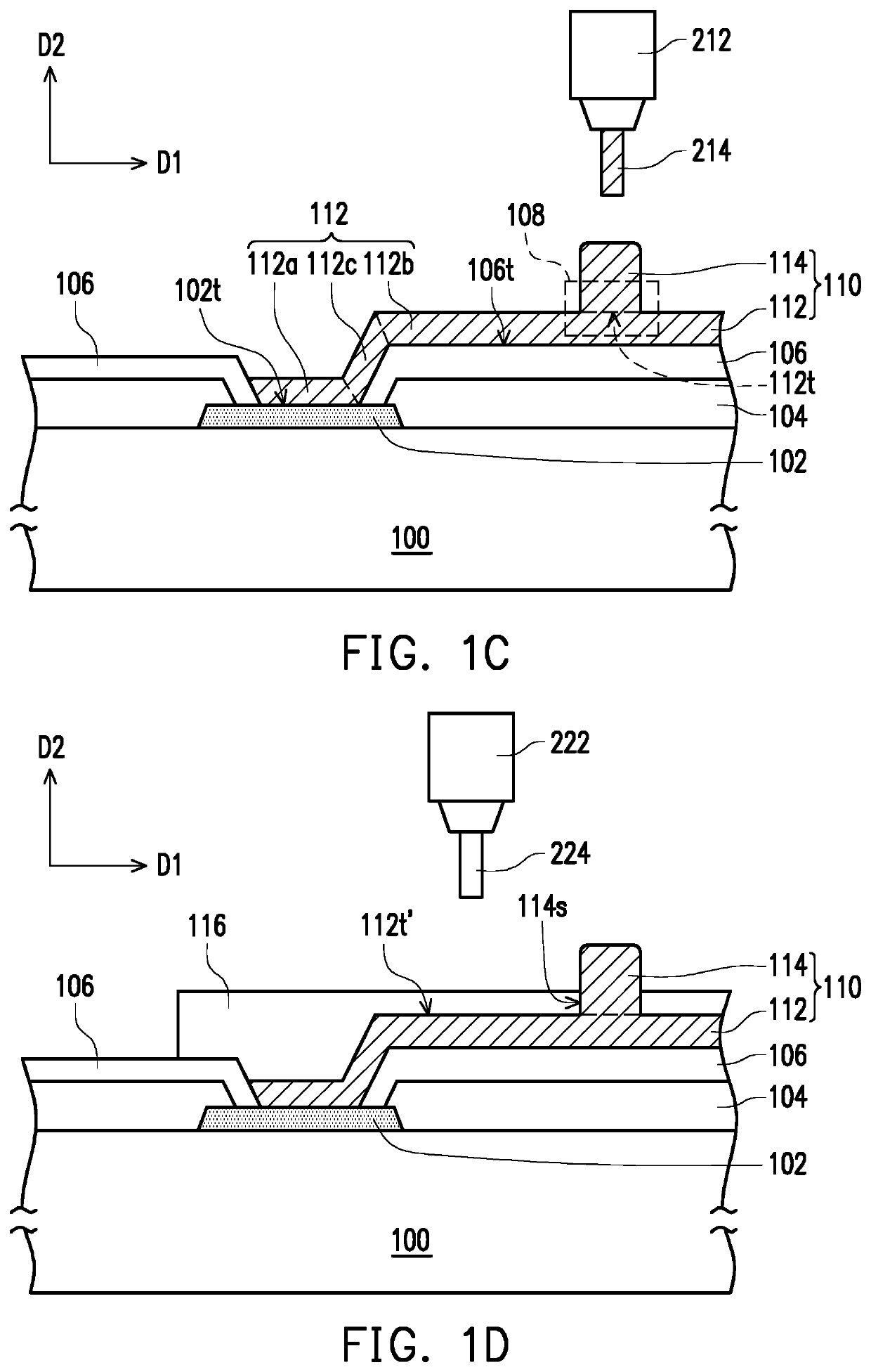
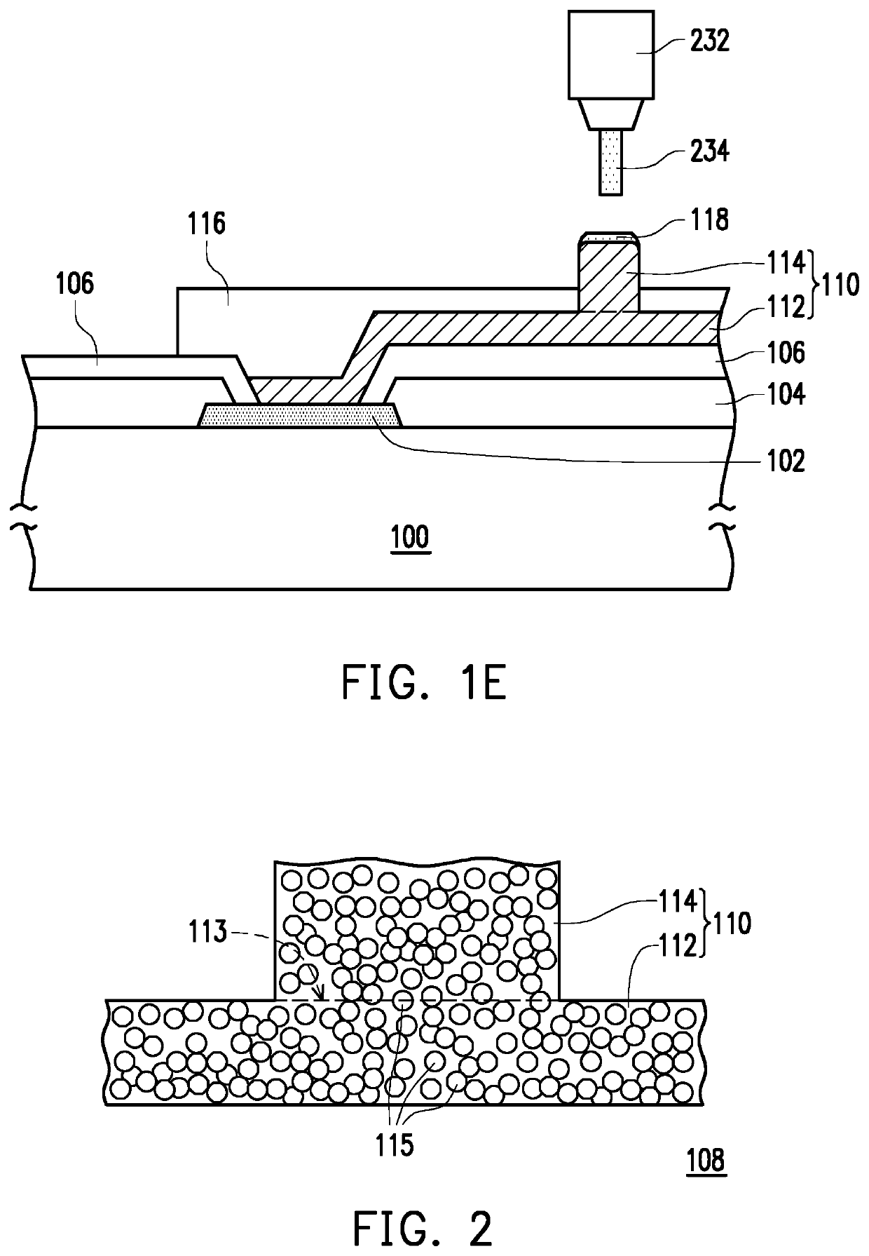
[0013]FIG. 1A to FIG. 1E are schematic cross-sectional views illustrating a manufacturing process of a circuit structure according to an embodiment of the disclosure. FIG. 2 is an enlarged cross-sectional view illustrating a portion of the circuit structure depicted in FIG. 1C. Here, the circuit structure provided in the present embodiment may be a redistribution layer (RDL) structure, which should however not be construed as a limitation in the disclosure. In other embodiments,...


PUM


Abstract

Provided is a circuit structure including a substrate, a pad, a dielectric layer, a conductive layer, an adhesion layer, and a conductive bump. The pad is disposed on the substrate. The dielectric layer is disposed on the substrate and exposes a portion of the pad. The conductive layer contacts the pad and extends from the pad to cover a top surface of the dielectric layer. The adhesion layer is disposed between the dielectric layer and the conductive layer. The conductive bump extends in an upward manner from a top surface of the conductive layer. The conductive bump and the conductive layer are integrally formed. A method of manufacturing the circuit structure is also provided.

Description

BACKGROUNDTechnical Field[0001]The disclosure relates to a semiconductor structure and a method of manufacturing the same, and more particularly to a circuit structure and a method of manufacturing the same.Description of Related Art[0002]Recently, the continuous increase in the integration of various electronic components (e.g., transistors, diodes, resistors, capacitors, and so on) leads to the rapid growth of the semiconductor industry. The increase in the integration mostly results from the continuous reduction of the minimum feature size, so that more components can be integrated into a given area.[0003]Compared to the convention package structure, these electronic components with smaller size occupy smaller area and thus require a smaller package structure. For instance, a semiconductor chip or die has an increasing number of input / output (I / O) solder pads, and a redistribution layer (RDL) can redistribute the original I / O solder pads of the semiconductor chip or die to be loc...

Claims


Application Information

Patent Timeline
IPC IPC(8): H01L23/00
CPCH01L2224/13008H01L24/13H01L2224/13564H01L2224/1132H01L2224/13247H01L2224/13239H01L24/11H01L2224/05548H01L2224/0401H01L2224/02311H01L2224/03332H01L2224/03312H01L2224/0391H01L2224/11332H01L2224/11312H01L2224/1191H01L2224/13082H01L2224/11515H01L24/03H01L24/02H01L24/05H01L2224/05147H01L2224/13347H01L2224/13147H01L2224/05794H01L2224/13139H01L2224/05839H01L2224/05155H01L2224/05164H01L2224/13111H01L2224/05144H01L2224/05847H01L2224/13339H01L2224/131H01L2224/05139H01L2224/05124H01L2224/13294H01L2924/00014H01L2924/013H01L2924/01047H01L2924/014H01L2924/01029H01L2924/0105
Inventor WU, JIN-NENGCHU, YEN-JUI
Owner WINBOND ELECTRONICS CORP
Why Eureka
Try Eureka