Ceramic electronic device, circuit substrate and manufacturing method of ceramic electronic device

Active Publication Date: 2020-10-22
TAIYO YUDEN KK
View PDF5 Cites 0 Cited by
  • Summary
  • Abstract
  • Description
  • Claims
  • Application Information

AI Technical Summary

Benefits of technology

The present invention aims to provide a ceramic electronic device that has improved resistance to humidity, voltage, and reliability. The invention solves the issue of a large cavity occurring among the external electrodes, internal electrode layers, and dielectric layers when the thicknesses of the external electrodes are reduced to improve the capacity volume density of the ceramic electronic device.

Problems solved by technology

However, in the ceramic electronic device in which Ni internal electrode layers and Cu external electrodes are used, a large amount of Cu of the external electrodes diffuse into the internal electrode layers during firing of the external electrodes (for example, see Japanese Patent Application Publication No. 2014-241453).
Therefore, resistance to humidity, resistance to voltage and reliability may be degraded.

Method used


Image

  • Ceramic electronic device, circuit substrate and manufacturing method of ceramic electronic device
  • Ceramic electronic device, circuit substrate and manufacturing method of ceramic electronic device
  • Ceramic electronic device, circuit substrate and manufacturing method of ceramic electronic device

Examples


embodiment

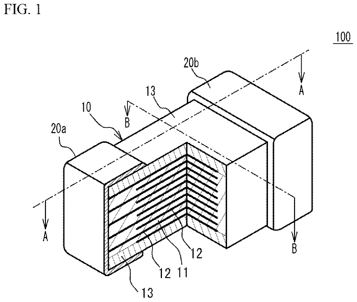
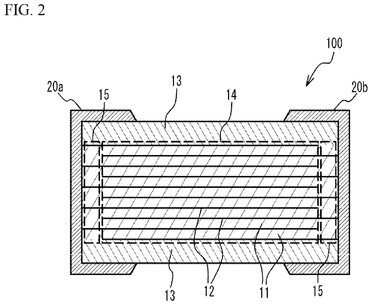
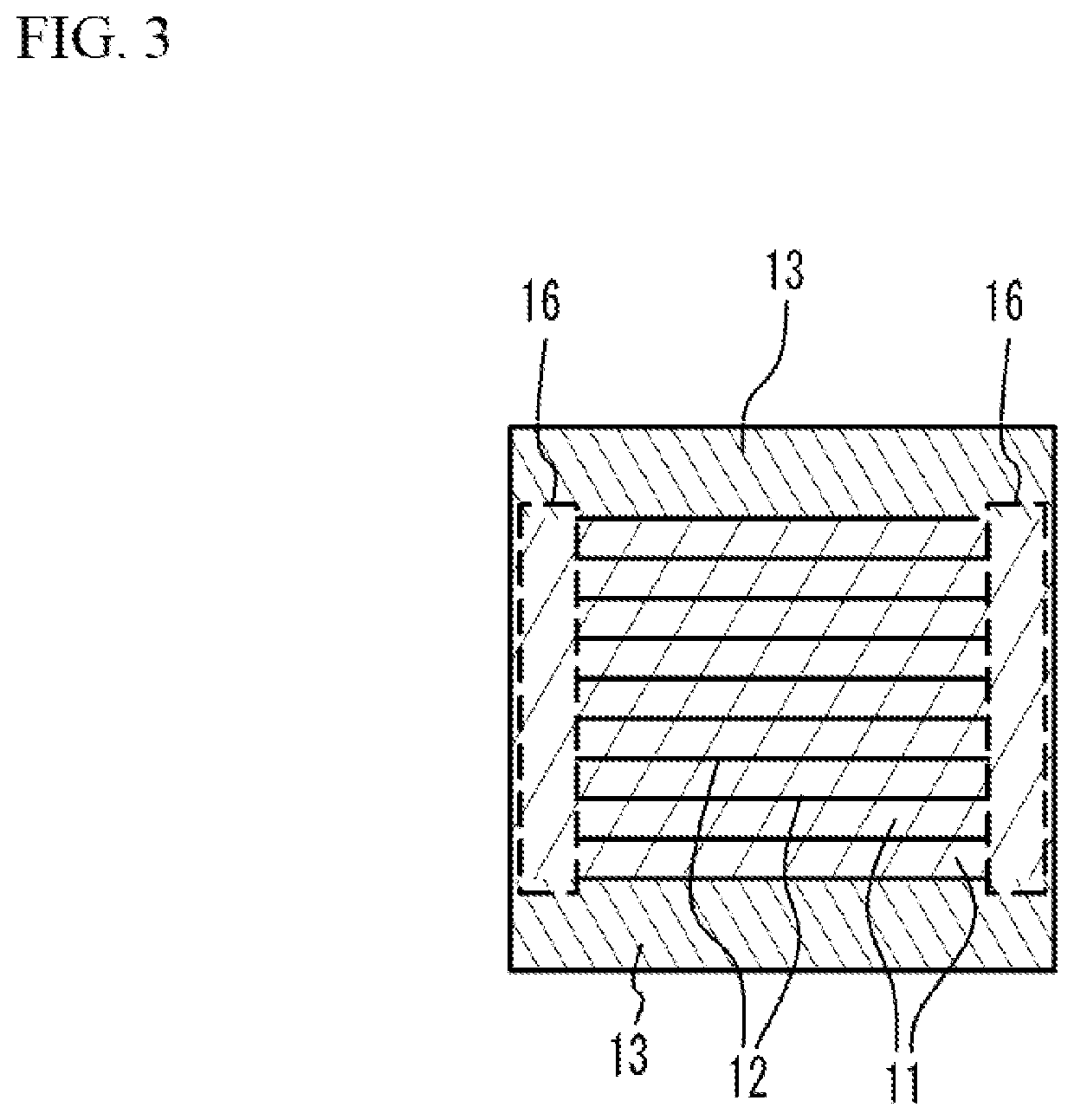
[0021]A description will be given of an outline of a multilayer ceramic capacitor, as an example of a ceramic electronic device. FIG. 1 illustrates a perspective view of a multilayer ceramic capacitor 100 in accordance with an embodiment, in which a cross section of a part of the multilayer ceramic capacitor 100 is illustrated. FIG. 2 illustrates a cross sectional view taken along a line A-A of FIG. 1. FIG. 3 illustrates a cross sectional view taken along a line B-B of FIG. 1. As illustrated in FIG. 1 to FIG. 3, the multilayer ceramic capacitor 100 includes a multilayer chip 10 having a rectangular parallelepiped shape, and a pair of external electrodes 20a and 20b that are respectively provided at two end faces of the multilayer chip 10 facing each other. In four faces other than the two end faces of the multilayer chip 10, two faces other than an upper face and a lower face of the multilayer chip 10 in a stacking direction are referred to as side faces. The external electrodes 20a...

examples

[0062]The multilayer ceramic capacitors in accordance with the embodiment were made and the property was measured.


PUM


Abstract

A ceramic electronic device includes: a multilayer chip having a structure in which each of dielectric layers and each of internal electrode layers are alternately stacked; and external electrodes provided on end faces of the multilayer chip, wherein a main component of the external electrodes is a first metal, wherein the internal electrode layers include the first metal and a second metal of which a melting point is higher than that of the first metal, wherein a diffusion coefficient of the first metal with respect to the second metal is larger than that of the second metal with respect to the first metal, wherein a number of a cavity in a range of 10 numbers of the internal electrode layers that are next to each other and are connected to a same external electrode of the first external electrode and the second external electrode is 1 or less.

Description

CROSS-REFERENCE TO RELATED APPLICATION[0001]This application is based upon and claims the benefit of priority of the prior Japanese Patent Application No. 2019-081284, filed on Apr. 22, 2019 and Japanese Patent Application No. 2020-016251, filed on Feb. 3, 2020, the entire contents of which are incorporated herein by reference.FIELD[0002]A certain aspect of the present invention relates to a ceramic electronic device, a circuit substrate and a manufacturing method of the ceramic electronic device.BACKGROUND[0003]Ceramic electronic devices such as multilayer ceramic capacitors have a high capacity density. Therefore, the ceramic electronic devices are widely used for electronic devices. Generally, Cu (copper) is used as external electrodes. A favorable sintering temperature of Cu is different from a favorable sintering temperature of dielectric layers. Therefore, exposed parts of internal electrodes are coated with paste Cu material and the paste Cu material is fired, after a ceramic...

Claims


Application Information

Patent Timeline
IPC IPC(8): H01G4/008H01G4/30H01G4/248H01G4/012H01G4/232
CPCH01G4/232H01G4/008H01G4/30H01G4/248H01G4/012H01G4/0085
Inventor TANAKA, TAKEHIROMIZUNO, KOTAROKOWASE, YUSUKE
Owner TAIYO YUDEN KK
Why Eureka
Try Eureka