Composite sintered body, semiconductor manufacturing apparatus member, and method of manufacturing composite sintered body

a technology of semiconductor manufacturing apparatus and composite sintered body, which is applied in the direction of manufacturing tools, inorganic insulators, work holders, etc., can solve the problems of increasing the amount of corrosion per unit time, generating undesired particles, and further falling off, so as to reduce the abnormal growth of aluminum oxide, reduce the amount of corrosion, and reduce the effect of tan

Pending Publication Date: 2020-11-05
NGK INSULATORS LTD
View PDF5 Cites 1 Cited by
  • Summary
  • Abstract
  • Description
  • Claims
  • Application Information

AI Technical Summary

Benefits of technology

[0013]The present invention is intended for a composite sintered body, and it is an object of the present invention to suppress the abnormal grain growth of aluminum oxide and provide a composite sintered body having high relative dielectric constant and withstand voltage, and low tan δ.

Problems solved by technology

In the dielectric material disclosed in Documents 1 and 2, however, since the particle diameter of SiC having relatively low corrosion resistance is small and the particle diameter of Al2O3 is also small, unevenness in a surface of the electrostatic chuck becomes prominent with corrosion and fall-off of SiC and this causes further fall-off of particles, and therefore there is a possibility that the amount of corrosion per unit time may increase.
Further, there is also a possibility that the Al2O3 particles may be desorbed from the electrostatic chuck during adsorption of the semiconductor substrate or the like, to thereby generate undesired particles.
Further, the value of the withstand voltage is not sufficiently high, and when the dielectric material is used for the electrostatic chuck of the above-described etching apparatus, there is a possibility of causing dielectric breakdown.
Since the SiC particles are fine and highly dispersed in the dielectric material, the SiC particles are easy to become a conductive path, and it is difficult to increase the withstand voltage.
Furthermore, since the SiC particles are fine, it is estimated that the sinterability of the dielectric material is reduced, and it is thought that closed pores which are thereby generated also make it difficult to reduce the tan δ and increase the withstand voltage.
Therefore, there is a limit to suppression of the abnormal grain growth of Al2O3.

Method used


Image

  • Composite sintered body, semiconductor manufacturing apparatus member, and method of manufacturing composite sintered body
  • Composite sintered body, semiconductor manufacturing apparatus member, and method of manufacturing composite sintered body
  • Composite sintered body, semiconductor manufacturing apparatus member, and method of manufacturing composite sintered body

Examples


Embodiment Construction

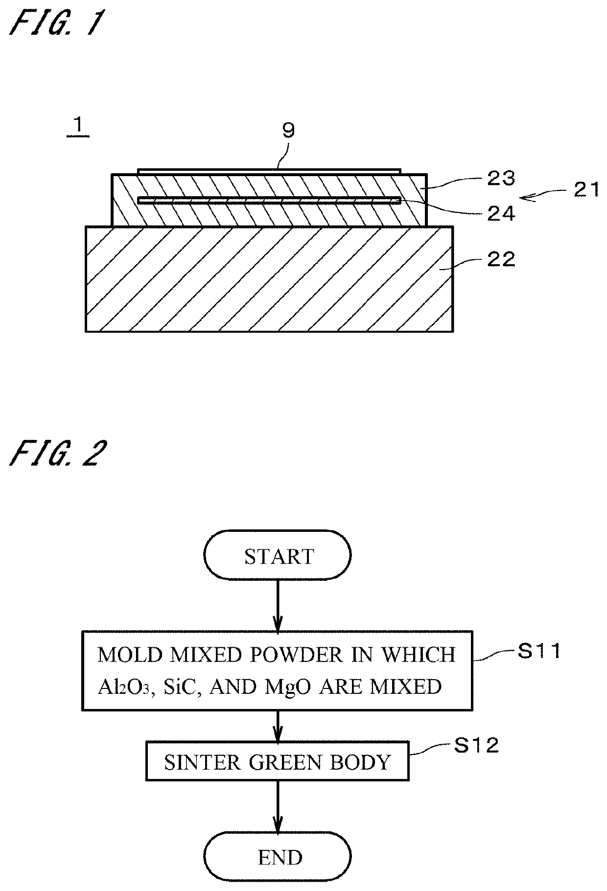
[0042]FIG. 1 is a cross section showing an electrostatic chuck 1 in accordance with one preferred embodiment of the present invention. The electrostatic chuck 1 is a semiconductor manufacturing apparatus member used in a semiconductor manufacturing apparatus. The electrostatic chuck 1 holds a substantially disk-like semiconductor substrate (hereinafter, referred to simply as a “substrate 9”) by electrostatically adsorption using the Coulomb force or the Johnsen-Rahbek force.

[0043]The electrostatic chuck 1 includes a chuck part 21 and a base part 22. The chuck part 21 is a member having a substantially disk-like shape. The chuck part 21 is attached on the base part 22. The chuck part 21 includes a chuck body 23 and an internal electrode 24. The chuck body 23 is a member which has a substantially disk-like shape and is formed of a composite sintered body. On an upper surface of the chuck body 23, placed is a substrate 9. The internal electrode 24 is an electrode disposed inside the ch...


PUM

PropertyMeasurementUnit
particle diameteraaaaaaaaaa

Abstract

A method of manufacturing a composite sintered body includes a step (Step S11) of molding mixed powder in which Al2O3, SiC, and MgO are mixed, into a green body having a predetermined shape and a step (Step S12) of generating a composite sintered body by sintering the green body. Then, in Step S11, the ratio of SiC to the mixed powder is not lower than 4.0 weight percentage and not higher than 13.0 weight percentage. Further, the purity of Al2O3 in Step S11 is not lower than 99.9%. It is thereby possible to suppress the abnormal grain growth of Al2O3 and suitably manufacture a composite sintered body having high relative dielectric constant and withstand voltage, and low tan δ.

Description

CROSS REFERENCE TO RELATED APPLICATION[0001]The present application claims priority to International Patent Application PCT / JP 2019 / 005853 filed on Feb. 18, 2019, the content of which is incorporated herein by reference in its entirety.TECHNICAL FIELD[0002]The present invention relates to a composite sintered body, a semiconductor manufacturing apparatus member, and a method of manufacturing a composite sintered body.BACKGROUND ART[0003]In an apparatus of manufacturing a semiconductor substrate or the like, conventionally, used is a susceptor such as an electrostatic chuck which holds a semiconductor substrate by adsorption using the Coulomb force or the Johnsen-Rahbek force, a heater which increases the temperature of a semiconductor substrate, an electrostatic chuck heater combining the electrostatic chuck and the heater, or the like. The electrostatic chuck includes a main body having a substantially disk-like shape, on which a semiconductor substrate is placed, and an internal e...

Claims


Application Information

Patent Timeline
Patent Type & Authority Applications(United States)
IPC IPC(8): H01L21/683B28B1/00C04B35/117C04B35/565
CPCC04B35/117B28B1/001C04B35/565H01L21/6833B25B11/00H01B3/12H01L21/6831H01L21/68757H01L21/67103C04B2235/3206C04B2235/77C04B2235/786C04B2235/96C04B2235/72C04B2235/3834C04B2235/5436C04B2235/5463C04B2235/3217C04B2235/5445C04B35/645C04B35/622H01L21/683C04B2235/3826
Inventor NAGAI, ASUMIINOUE, KATSUHIROKATSUDA, YUJI
Owner NGK INSULATORS LTD
Why Eureka
Try Eureka