
Highly selective silicon oxide/silicon nitride etching by selective boron nitride or aluminum nitride deposition

a technology of silicon oxide and nitride, which is applied in the direction of semiconductor/solid-state device manufacturing, basic electric elements, electric apparatus, etc., can solve the problems of huge challenge in the development of advanced semiconductor technology

Active Publication Date: 2020-12-24
TOKYO ELECTRON LTD
View PDF0 Cites 1 Cited by
  • Summary
  • Abstract
  • Description
  • Claims
  • Application Information

AI Technical Summary

Benefits of technology

This patent describes a method for selectively etching silicon oxide relative to silicon nitride on a substrate. The method involves exposing the substrate to two different gases, one of which contains boron or aluminum, to form two layers of different nitrides on the substrate. The second layer of nitride protects the silicon nitride film from etching by an etching gas. A third gas is then used to etch the first nitride layer and the silicon oxide film, while the second nitride layer protects the silicon nitride film. The method also involves exposing the substrate to a gas that contains hydrogen to terminate the silicon oxide film and the silicon nitride film with different surface species. Overall, this method allows for selective etching of silicon oxide without damaging the silicon nitride film on a substrate.

Problems solved by technology

Advanced semiconductor technology development poses a huge challenge as dry etch removal of one material selective to other materials is needed.

Method used


Image

  • Highly selective silicon oxide/silicon nitride etching by selective boron nitride or aluminum nitride deposition
  • Highly selective silicon oxide/silicon nitride etching by selective boron nitride or aluminum nitride deposition
  • Highly selective silicon oxide/silicon nitride etching by selective boron nitride or aluminum nitride deposition

Examples


Embodiment Construction

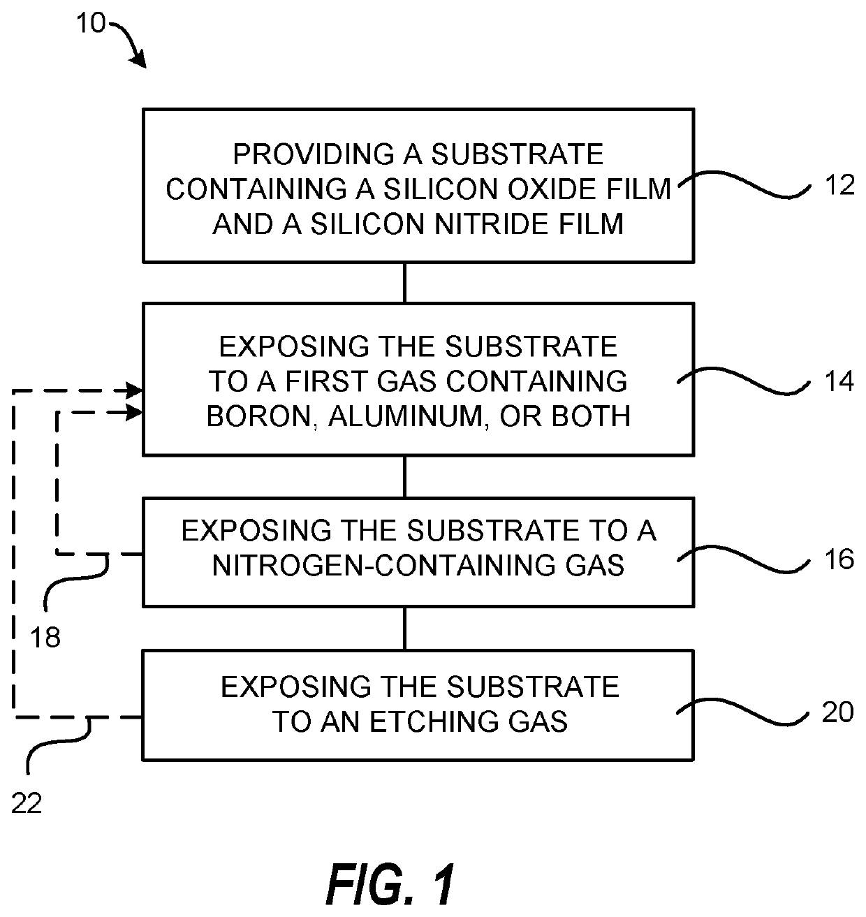
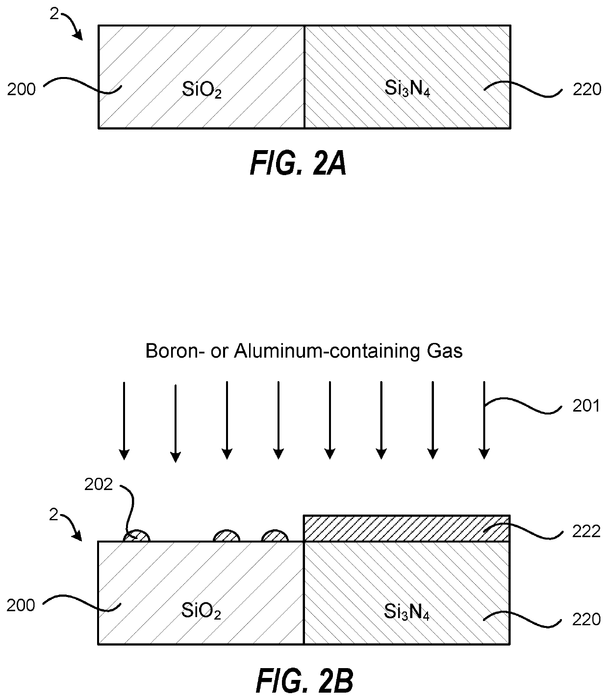
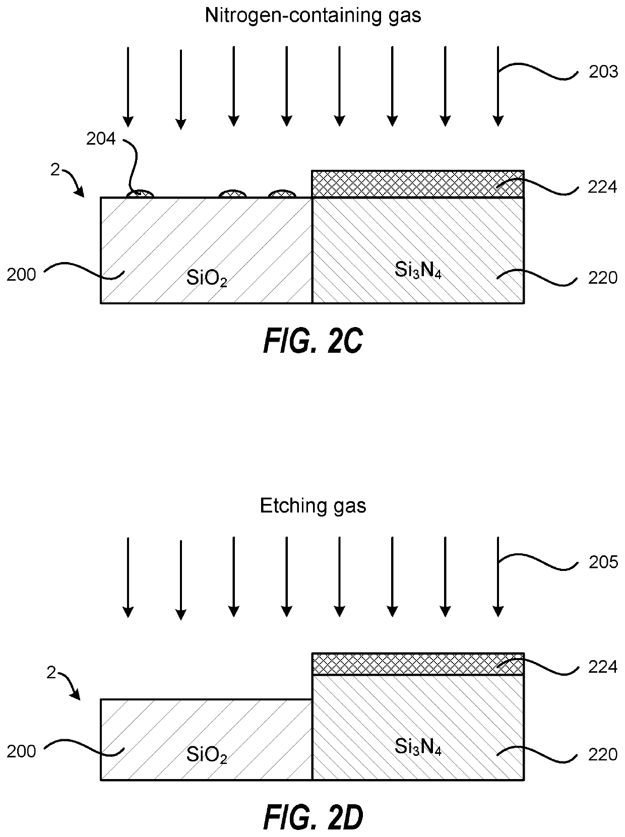
[0011]FIG. 1 is a process flow diagram for selective etching of a silicon oxide film relative to a silicon nitride film according to an embodiment of the invention, and FIGS. 2A-2D schematically show through cross-sectional views a method of selective etching of a silicon oxide film relative to a silicon nitride film according to an embodiment of the invention.

[0012]Referring now to FIGS. 1 and 2A, the processing method in the process flow diagram 10 includes, in 12, providing a substrate 2 containing a SiO2 film 200 and a Si3N4 film 220. In the example shown in FIG. 2A, the SiO2 film 200 and the Si3N4 film 220 are in the same horizontal plane, but embodiments of the invention may also be applied to films that are not in the same horizontal plane but are offset vertically. Si3N4 is the most thermodynamically stable of the silicon nitrides and hence the most commercially important of the silicon nitrides. However, embodiments of the invention may be applied to other silicon nitrides ...


PUM


Abstract

A method for selective etching of silicon oxide relative to silicon nitride includes exposing a substrate to a first gas that forms a first layer on the silicon oxide film and a second layer on the silicon nitride film, where the first gas contains boron, aluminum, or both boron and aluminum, exposing the substrate to a nitrogen-containing gas that reacts with the first layer to form a first nitride layer on the silicon oxide film and reacts with the second layer to form a second nitride layer on the silicon nitride film, where a thickness of the second nitride layer is greater than a thickness of the first nitride layer. The method further includes exposing the substrate to an etching gas that etches the first nitride layer and silicon oxide film, where the second nitride layer protects the silicon nitride film from etching by the etching gas.

Description

CROSS-REFERENCE TO RELATED APPLICATIONS[0001]This application is related to and claims priority to U.S. Provisional Patent Application Ser. No. 62 / 864,378 filed on Jun. 20, 2019, the entire contents of which are herein incorporated by reference.FIELD OF INVENTION[0002]The present invention relates to the field of semiconductor manufacturing and semiconductor devices, and more particularly, to a method of selective etching of silicon oxide relative to silicon nitride.BACKGROUND OF THE INVENTION[0003]Advanced semiconductor technology development poses a huge challenge as dry etch removal of one material selective to other materials is needed. Selective silicon oxide etching relative to silicon nitride has many applications in semiconductor manufacturing and preferential passivation (mostly carbon-based) has been extensively explored for high etch selectivity when using plasmas containing fluorocarbon (FC) or hydrofluorocarbon (HFC) gases. The need for high etch selectivity is especial...

Claims


Application Information

Patent Timeline
IPC IPC(8): H01L21/306H01L21/3105
CPCH01L21/31055H01L21/30621H01L21/31116H01L21/31144H01L21/02175H01L21/02178H01L21/02252H01L21/0228
Inventor TSAI, YU-HAOZHANG, DUWANG, MINGMEI
Owner TOKYO ELECTRON LTD
Learn More