
Memory systems for performing failover

Active Publication Date: 2021-01-28
SAMSUNG ELECTRONICS CO LTD
View PDF0 Cites 21 Cited by
  • Summary
  • Abstract
  • Description
  • Claims
  • Application Information

AI Technical Summary

Benefits of technology

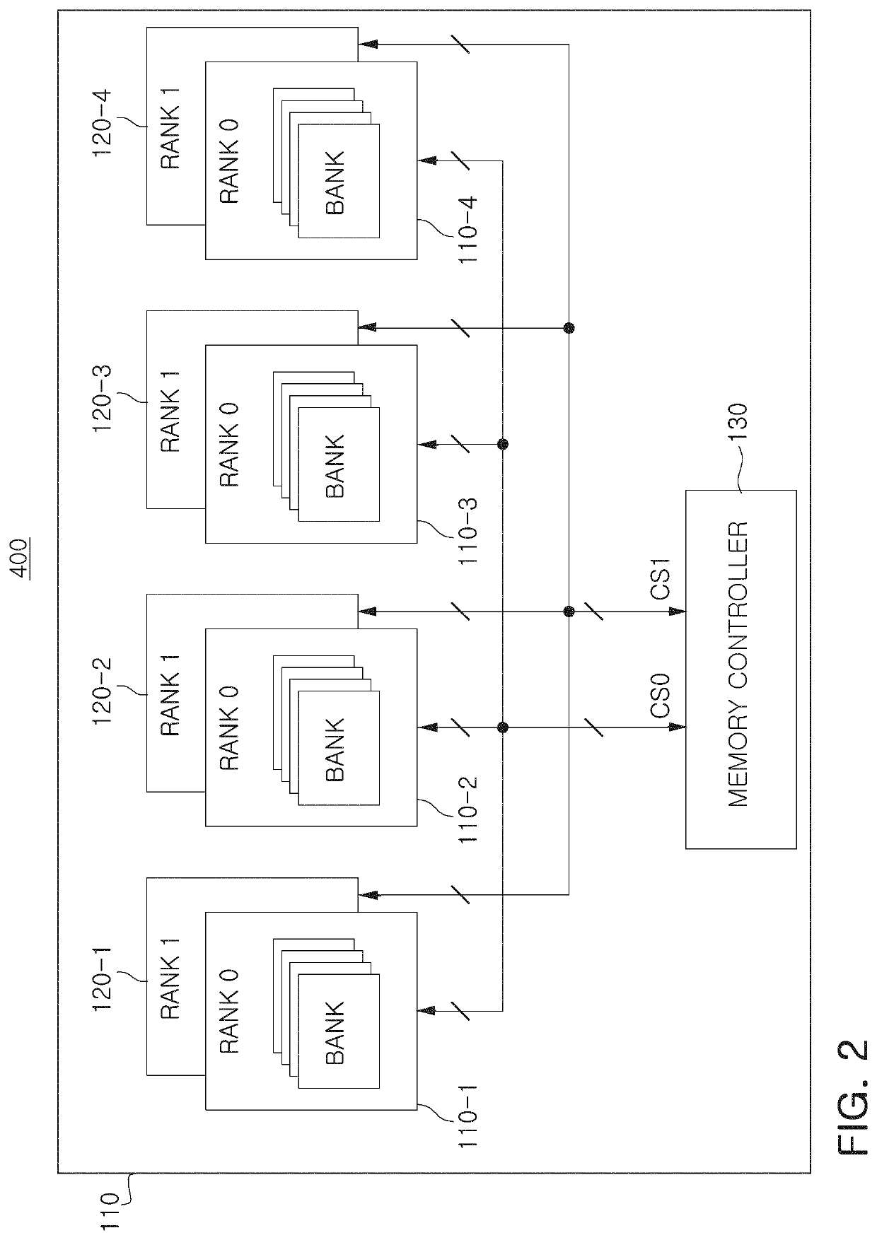
The present invention provides a memory system that can perform a failover function before an uncorrectable error correction code (UECC) occurs. The system includes multiple memory devices with redundant regions connected to a memory controller. The controller stores data in selected memory cells and the redundant region, replacing a selected word line with a redundancy word line in response to a CECC occurring in at least one of the selected memory cells. Additionally, the invention includes a memory module with two ranks of memory devices and a memory controller that activates chip select signals to write data to both ranks simultaneously. This results in faster data transfer and improved performance of the memory system.

Problems solved by technology

Due to a microfabrication process for a memory device such as a DRAM, a SRAM, and a flash memory, the number of defective memory cells included in the memory devices is increasing exponentially.

Method used


Image

  • Memory systems for performing failover
  • Memory systems for performing failover
  • Memory systems for performing failover

Examples


Embodiment Construction

[0025]Hereinafter, some example embodiments of the present inventive concepts will be described in detail with reference to the attached drawings.

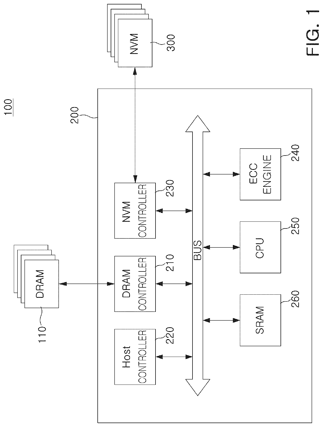
[0026]FIG. 1 is a schematic block diagram illustrating a memory system according to an example embodiment of the present disclosure.

[0027]Referring to FIG. 1, a memory system 100 includes a first memory module 110, a memory controller 200, and / or a second memory module 300. The first memory module 110, the memory controller 200, and the second memory module 300 may be integrated into a single semiconductor device. For example, first memory module 110, the memory controller 200, and the second memory module 300 may be integrated into a single semiconductor device to form a solid state drive (SSD).

[0028]The first memory module 110 may include a volatile memory such as DRAM, synchronous DRAM (SDRAM), double data rate (DDR) SDRAM, low-power DDR (LPDDR) SDRAM, SRAM, and / or the like, and / or a nonvolatile memory such as FRAM, ReRAM, STT-MRAM, PRA...


PUM


Abstract

A memory system includes a plurality of memory devices, each of the plurality of memory devices including a plurality of memory cells, and at least one of the plurality of memory devices including a backup region, and a memory controller configured to store data to be stored in a plurality of selected memory cells in the plurality of selected memory cells and the backup region, the plurality of selected memory cells being connected to a selected word line of a selected memory device among the plurality of memory devices, and replace the selected word line with a redundancy word line to which a plurality of redundancy memory cells among the plurality of memory cells are connected in response to a correctable error correction code (CECC) occurring in at least one of the plurality of selected memory cells.

Description

CROSS-REFERENCE TO RELATED APPLICATION(S)[0001]This application claims benefit of priority to Korean Patent Application No. 10-2019-0089434 filed on Jul. 24, 2019 in the Korean Intellectual Property Office, the disclosure of which is incorporated herein by reference in its entirety.BACKGROUND1. Field[0002]The present inventive concepts relate to a memory system.2. Description of Related Art[0003]The nonvolatile memory device may retain data stored in the nonvolatile memory device even when external power supply is interrupted. For example, a flash memory device is a nonvolatile memory device in which a programming operation and an erasing operation can be electrically performed. The flash memory device may be classified as a NAND-type flash memory or a NOR-type flash memory.[0004]Volatile memory uses a constant power supply to maintain stored information. Most random access memory (RAM) for general purposes, including a dynamic RAM (DRAM) and a static RAM (SRAM), is volatile memory....

Claims


Application Information

Patent Timeline
IPC IPC(8): G06F11/10G06F11/14G06F11/07G11C11/408G11C29/42G11C29/00
CPCG06F11/1044G06F11/1068G06F11/108G06F11/1469G11C29/78G06F11/076G11C11/4085G11C29/42G06F11/1456G06F11/2041G06F11/2094G11C11/408G11C11/4076G11C11/418G11C29/4401G06F11/1048G06F11/1666G06F11/2017G06F3/0604G06F3/0658G06F3/0619
Inventor PARK, INHOONKIM, DONGEUN, HYUNGLAELIM, CHULSEUNGJUNG, WONYEOUNG
Owner SAMSUNG ELECTRONICS CO LTD
Learn More