Charged Particle Beam System and Overlay Shift Amount Measurement Method

Pending Publication Date: 2021-02-25
HITACHI HIGH-TECH CORP
View PDF0 Cites 6 Cited by
  • Summary
  • Abstract
  • Description
  • Claims
  • Application Information

AI Technical Summary

Benefits of technology

[0011]According to the present invention, it is possible to provide a charged particle beam system and

Problems solved by technology

However, with the progress of miniaturization of patterns, it becomes difficult to obtain required detection accuracy using a method of detecting a shift amount with light.
As a result, there may be a problem that accurate information on the shape of the upper layer cannot be obtained.
However, if the number of

Method used


Image

  • Charged Particle Beam System and Overlay Shift Amount Measurement Method
  • Charged Particle Beam System and Overlay Shift Amount Measurement Method
  • Charged Particle Beam System and Overlay Shift Amount Measurement Method

Examples


first embodiment

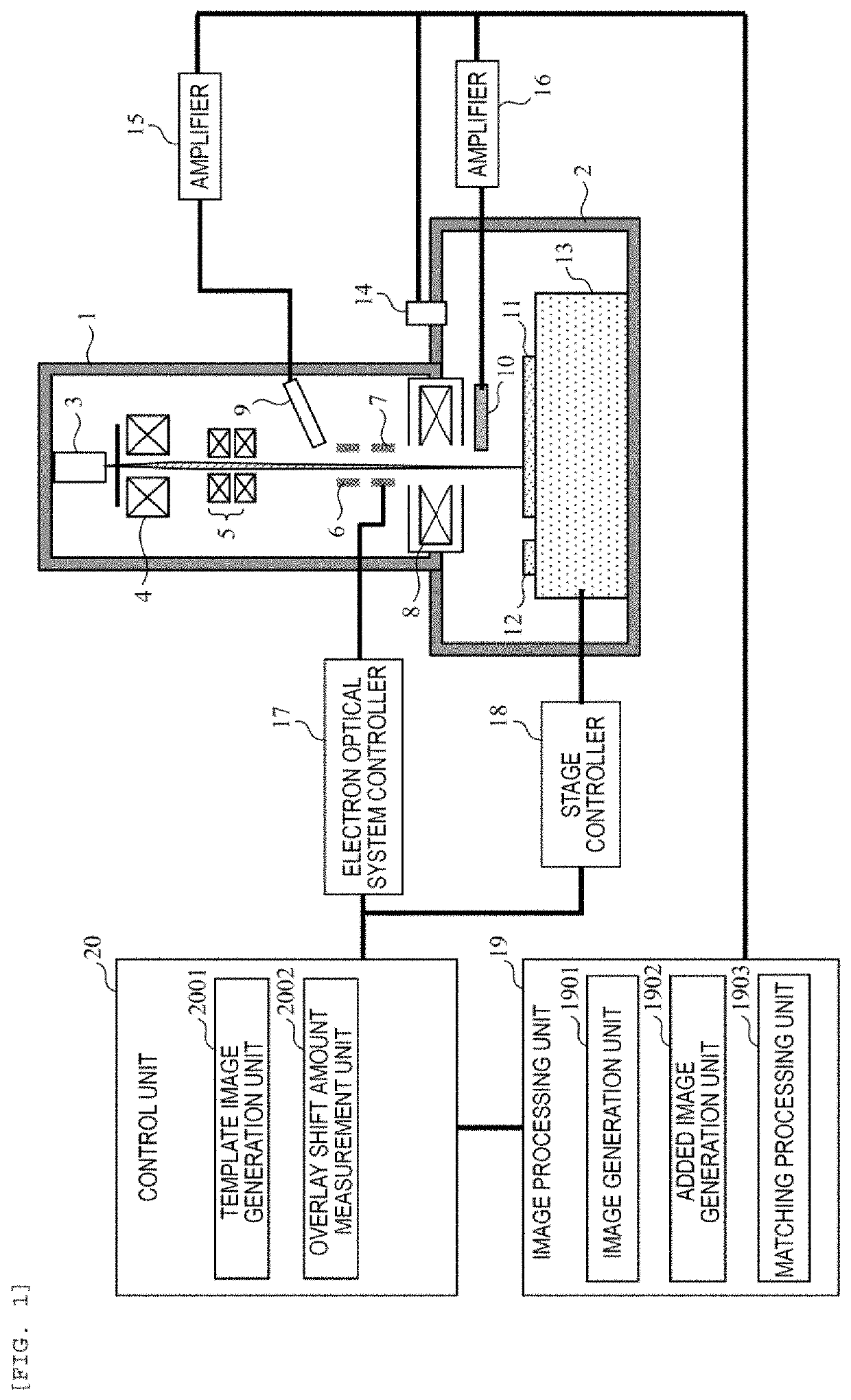
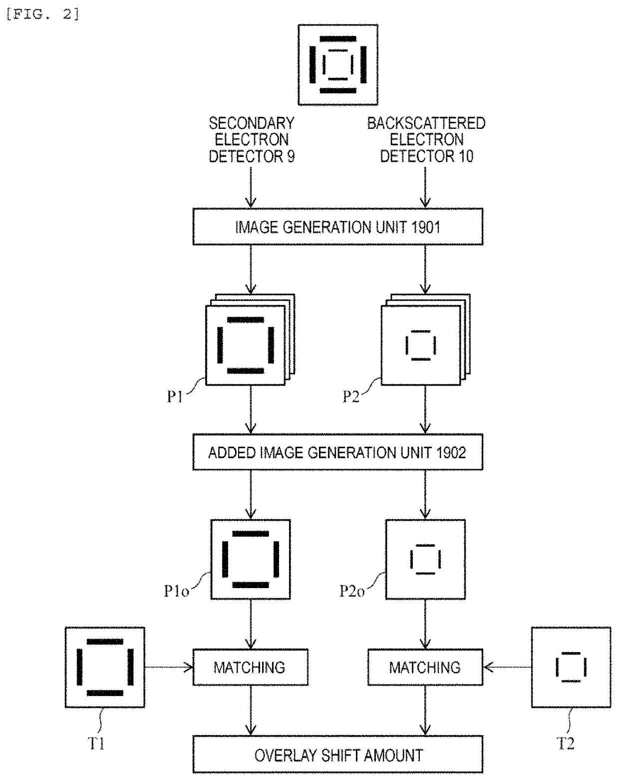
[0030]Referring to FIGS. 1 and 2, according to the first embodiment, a charged particle beam system including an overlay shift amount measuring function is described. This charged particle beam system is, for example, a scanning electron microscope (SEM) and is configured to be able to perform a method of measuring an overlay shift amount in which an overlay shift amount between an upper layer pattern and a lower layer pattern is measured by using an image acquired by the irradiation of electron beams which are charged particle beams. FIG. 1 is a schematic diagram illustrating a schematic configuration of a scanning electron microscope (SEM) of the first embodiment, and FIG. 2 is a schematic diagram illustrating operations of units.

[0031]The SEM includes a column 1 and a sample chamber 2 which are an electron optical system. The column 1 includes an electron gun 3 that generates electron beams (charged particle beams) for irradiation, a condenser lens 4, an aligner 5, an ExB filter ...

second embodiment

[0080]Next, a scanning electron microscope (SEM) as a charged particle beam system according to a second embodiment is described with reference to FIG. 11. The configuration of the scanning electron microscope according to the second embodiment may be substantially the same as that of the first embodiment (FIG. 1). The procedure of measuring an overlay shift amount can be also performed by the procedure which is substantially the same as that illustrated in the flowcharts of FIGS. 4 to 7. Here, according to the second embodiment, processes of an acquisition condition setting screen of Step S303c are different from those of the first embodiment.

[0081]According to the second embodiment, in the acquisition condition setting screen, a scanning method can be selected, and for example, bidirectional scanning can be selected as the scanning method. In other words, in the second embodiment, an added image can be generated by adding an image obtained by differentiating irradiation trajectori...

third embodiment

[0089]Subsequently, a scanning electron microscope (SEM) as a charged particle beam system according to a third embodiment is described with reference to FIG. 12. The configuration of the scanning electron microscope of the third embodiment may be substantially the same as that of the first embodiment (FIG. 1). The procedure of measuring an overlay shift amount can be performed through a procedure substantially the same as that illustrated in the flowcharts of FIGS. 4 to 7. Here, according to the third embodiment, in addition to a scanning method setting area 801, whether drift correction is to be performed (is required) can be selected.

[0090]In a scanning electron microscope, drift may occur due to charging of the target sample and affect the accuracy of the overlay shift measurement. For example, when a plurality of images are captured and added to generate an added image, if the target sample is charged by electron beam irradiation, the charge amount differs between the plurality...


PUM


Abstract

Overlay shift amount measurement with high accuracy becomes possible. A charged particle beam system includes a computer system that measures an overlay shift amount between a first layer of a sample and a second layer lower than the first layer based on output of a detector. The computer system generates first images with respect to the first layer and second images with respect to the second layer based on the output of the detector, generates a first added image by adding the first images by a first added number of images, and generates a second added image by adding the second image by a second added number of images greater than the first added number of images. An overlay shift amount between the first layer and the second layer is measured based on the first added image and the second added image.

Description

TECHNICAL FIELD[0001]The present invention relates to a charged particle beam system and an overlay shift amount measurement method.BACKGROUND ART[0002]A semiconductor device is manufactured by performing a process of transferring a pattern formed on a photomask onto a semiconductor wafer using lithography processing and etching processing and repeating this process. During the process of manufacturing a semiconductor device, the quality of lithography and etching processing, generation of foreign matters, and the like greatly affect the yield of semiconductor devices to be manufactured. Therefore, it is important to detect the occurrence of an abnormality or a defect in the manufacturing process early or in advance in order to improve the yield of semiconductor devices.[0003]Therefore, in the manufacturing process of a semiconductor device, a pattern formed on a semiconductor wafer is measured or inspected. Particularly, with the recent progress in miniaturization and three-dimensi...

Claims


Application Information

Patent Timeline
IPC IPC(8): G01B15/00G01N23/2251G01N23/203
CPCG01B15/00G01N23/2251G01N23/203G01N2223/045G01B2210/56G01N2223/071G01N2223/401G01N2223/6116G01N2223/053G03F7/70633H01J2237/221H01J37/28H01J2237/2817H01J37/222H01J37/244
Inventor YAMAKI, TAKUMAYAMAMOTO, TAKUMAGOTO, YASUNORITAMORI, TOMOHIROASAO, KAZUNARI
Owner HITACHI HIGH-TECH CORP
Why Eureka
Try Eureka