Organic light emitting diode display device

a light-emitting diode and display device technology, which is applied in the direction of diodes, semiconductor devices, electrical apparatuses, etc., can solve the problems of difficult to increase the aperture ratio of the emission area, and achieve the effect of suppressing voltage drop, reducing resistance of the second electrode, and increasing refractive index

Active Publication Date: 2021-03-18
LG DISPLAY CO LTD
View PDF2 Cites 1 Cited by
  • Summary
  • Abstract
  • Description
  • Claims
  • Application Information

AI Technical Summary

Benefits of technology

[0006]Accordingly, the present disclosure is to provide a display device in which the transparency is improved by increasing a transmission area and a voltage drop of a second electrode is suppressed by simplifying the structure.
[0027]According to the aspects of the present disclosure, in an OLED display device, a conductive layer in contact with a second electrode of an OLED is connected to a conductive black matrix using a conductive fill material filled therebetween. Therefore, it is possible to reduce a resistance of the second electrode and thus suppress a voltage drop.
[0028]Further, according to the aspects of the present disclosure, the OLED display device includes the conductive layer whose refractive index can be easily controlled by adjusting the composition ratio. The conductive layer may have a higher refractive index than the second electrode. Therefore, it is possible to reduce total reflection of light and thus possible to improve the luminous efficiency.
[0029]Further, according to the aspects of the present disclosure, the OLED display device does not include a cathode contact portion. Thus, it is possible to increase the size of a transmission area and thus possible to improve the transmittance.

Problems solved by technology

Thus, it is difficult to increase the aperture ratio of the emission area.

Method used


Image

  • Organic light emitting diode display device
  • Organic light emitting diode display device
  • Organic light emitting diode display device

Examples


Embodiment Construction

[0045]Hereinafter, the exemplary aspects of the present disclosure will be described with reference to the accompanying drawings. Throughout the whole specification, the same reference numerals denote substantially the same elements. Further, in the following, a detailed explanation of known technologies or configurations related to the present disclosure may be omitted to avoid unnecessarily obscuring the subject matter of the present disclosure. Further, the names of elements used herein are chosen for ease of description and may be different from the names of parts used in actual products.

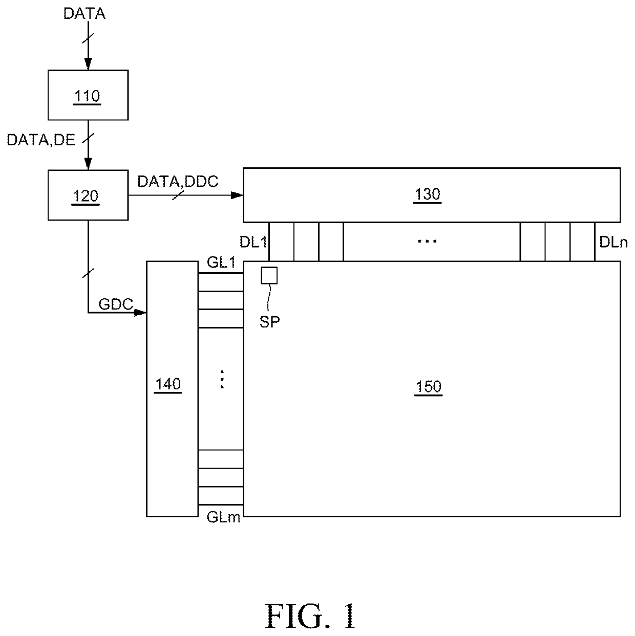
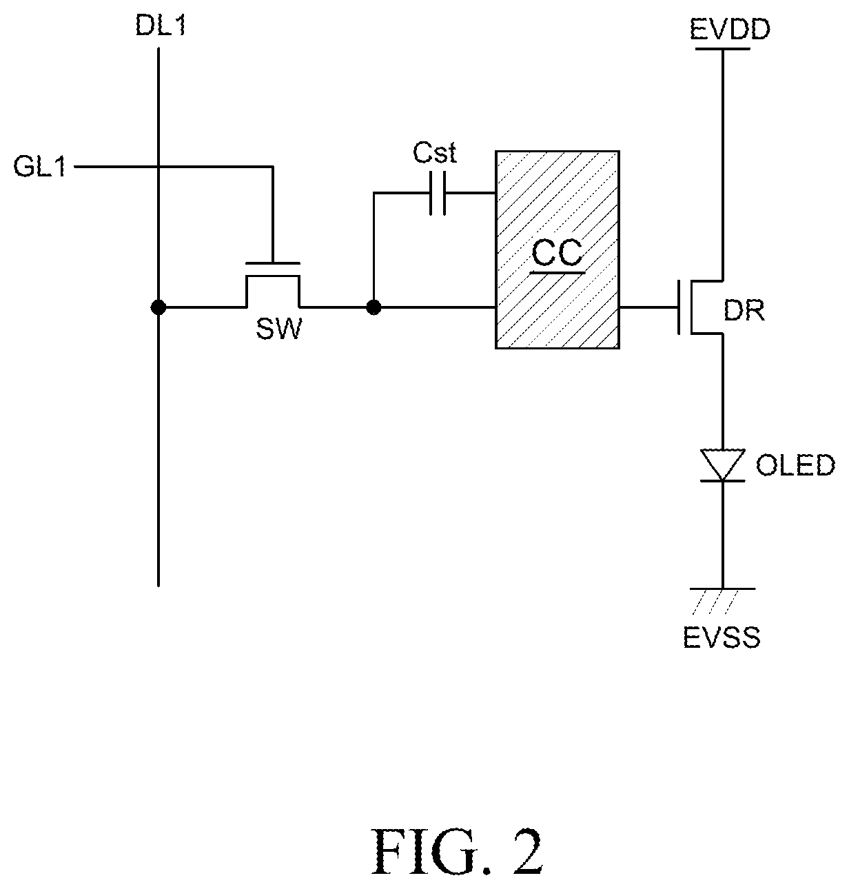
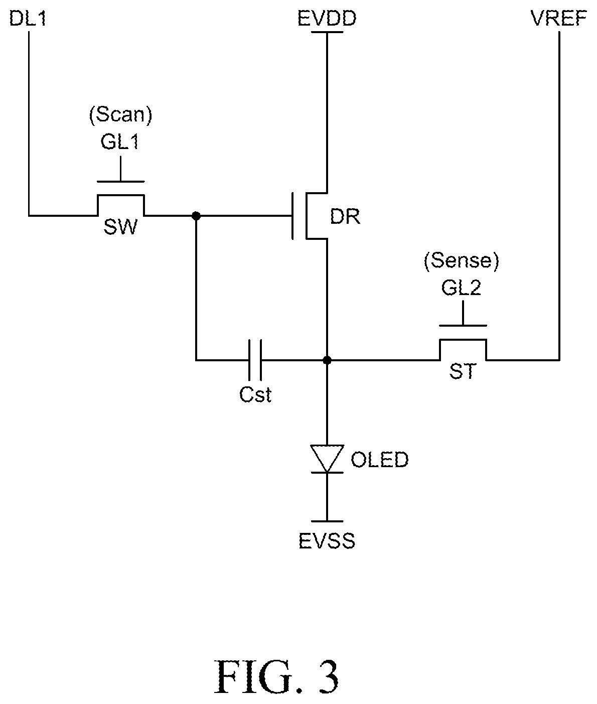
[0046]A display device according to the present disclosure may be an OLED display device, an LCD, an ED, and the like, but in the present disclosure, the OLED display device will be described as an example. The OLED display device includes a first electrode as an anode, a second electrode as a cathode, and an organic layer formed of an organic material between the first electrode and the second ...


PUM

PropertyMeasurementUnit
refractive indexaaaaaaaaaa

Abstract

An organic light emitting diode display device includes a first substrate, an organic light emitting diode including a first electrode, an organic layer and a second electrode and disposed on the first substrate, a conductive layer disposed on the organic light emitting diode, a second substrate disposed over the first substrate, a conductive black matrix disposed on a surface of the second substrate that faces the first substrate, a sealant boding the first substrate and the second substrate and a conductive fill material filled between the first substrate and the second substrate.

Description

CROSS-REFERENCE TO RELATED APPLICATION[0001]This application claims the priority of Korean Patent Application No. 10-2019-0114257 filed on Sep. 17, 2019, which is hereby incorporated by reference in its entirety.BACKGROUNDField of the Disclosure[0002]The present disclosure relates to an organic light emitting diode (OLED) display device, and more particularly, to an OLED display device in which the transparency is improved by increasing a transmission area and a voltage drop of a second electrode is suppressed by simplifying the structure.Description of the Background[0003]With the development of information society, various demands for display devices for displaying images are increasing. In the field of display devices, flat panel display devices (FPDs), which are thin, light, and can have a large area, have been rapidly replacing bulky cathode ray tubes (CRTs). Examples of the FPDs include a liquid crystal display device (LCD), a plasma display panel (PDP), an OLED display device...

Claims


Application Information

Patent Timeline
Patent Type & Authority Applications(United States)
IPC IPC(8): H01L51/52H01L27/32
CPCH01L51/5228H01L51/5246H01L27/3276H01L51/5275H01L27/322H01L27/3272H01L27/1218H10K59/122H10K59/131H10K50/82H10K59/38H10K59/123H10K59/121H10K59/1315H10K50/824H10K50/841H10K50/858H10K50/865H10K59/1201H10K2102/3026H10K71/861H10K50/805H10K50/84H10K50/8426H10K59/126
Inventor LEE, MIREUM
Owner LG DISPLAY CO LTD
Why Eureka
Try Eureka