Thermoelectric separation LED substrate and manufacturing method thereof

A LED substrate, thermoelectric separation technology, applied in the direction of circuits, electrical components, electric solid devices, etc., can solve the problem of poor lateral thermal conductivity of LED substrates, and achieve the effects of lower temperature, faster heat conduction rate, and improved heat dissipation

Pending Publication Date: 2020-01-14
厦门市信达光电科技有限公司
View PDF0 Cites 0 Cited by
  • Summary
  • Abstract
  • Description
  • Claims
  • Application Information

AI Technical Summary

Problems solved by technology

[0004] The present invention aims to provide a thermoelectrically separated LED substrate to solve the problem of poor lateral thermal conductivity of the existing LED substrate

Method used


Image

  • Thermoelectric separation LED substrate and manufacturing method thereof
  • Thermoelectric separation LED substrate and manufacturing method thereof
  • Thermoelectric separation LED substrate and manufacturing method thereof

Examples


Embodiment 1

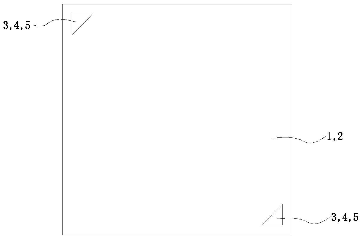
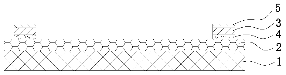
[0033] Such as figure 1 with figure 2 As shown, the present embodiment provides a thermally and electrically separated LED substrate, which includes a metal substrate, a graphene layer 2 bonded to the surface of the metal substrate, and at least two solder joints arranged on the graphene layer 2 Each pad 3 and the graphene layer 2 are insulated and isolated by an insulating layer 4 .

[0034] Specifically, the metal substrate is used to dissipate heat and provide support for the overall package structure. It has a front side and a back side opposite to each other. In this embodiment, the front side is used as a die-bonding surface. Among them, the metal substrate is preferably a copper substrate 1 with high thermal conductivity, so that the metal substrate has better heat dissipation performance. In this embodiment, the copper substrate 1 as the metal substrate is also taken as an example for illustration.

[0035] The graphene layer 2 can be grown on the surface of the co...

Embodiment 2

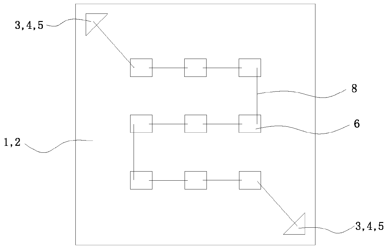
[0044] This embodiment provides a method for manufacturing the LED substrate in Embodiment 1, such as Image 6As shown, the manufacturing method includes the following steps:

[0045] A) Substrate fabrication, that is, growing a graphene layer 2 on the crystal-bonding surface of the copper substrate 1 . The graphene layer 2 is grown on the crystal-bonding surface of the copper substrate 1 by chemical vapor deposition (CVD), and covers the entire crystal-bonding surface of the copper substrate 1 . Specifically, gaseous carbon-containing compounds such as methane are used as carbon sources to grow graphene through pyrolysis on the surface of the substrate. Copper is a metal matrix with a low carbon solubility. Carbon atoms generated by the cracking of gaseous carbon sources at high temperatures are adsorbed on the metal surface and then nucleated and grown into graphene islands, and continuous graphite is obtained through the two-dimensional growth of graphene islands. ene fil...


PUM

PropertyMeasurementUnit
thermal conductivityaaaaaaaaaa

Abstract

The invention relates to a thermoelectric separation LED substrate and a manufacturing method thereof. The LED substrate comprises a metal substrate with a fixed surface, a graphene layer covering a whole solid crystal surface and at least two bonding pads fixed on the graphene layer, and each bonding pad and the graphene layer are insulated and isolated through an insulating layer, so that the problem of poor transverse heat conduction capability of the conventional LED substrate is solved.

Description

technical field [0001] The invention relates to the field of LED devices, in particular to a thermoelectrically separated LED substrate and a manufacturing method thereof. Background technique [0002] After years of development, LED lighting has become a very mature lighting technology. The LED device will generate a lot of heat in the working state, so that the temperature of the LED device will rise, and the high temperature will shorten the life of the LED and reduce the luminous performance of the LED. In order to prevent the LED temperature from being too high, an efficient heat dissipation method must be considered when designing the package structure. At present, most LED packaging manufacturers use materials with high thermal conductivity as the substrate, such as metal copper, aluminum, ceramics, etc., so that the heat generated by the chip is conducted to the environment through the substrate, and the thermal conductivity of copper and aluminum nitride ceramics e...

Claims


Application Information

Patent Timeline
Patent Type & Authority Applications(China)
IPC IPC(8): H01L23/14H01L33/64H01L33/62
CPCH01L23/142H01L33/62H01L33/64
Inventor 陈亚勇杨恩茂
Owner 厦门市信达光电科技有限公司
Why Eureka
Try Eureka