Unit cell and power amplifier module
- Summary
- Abstract
- Description
- Claims
- Application Information
AI Technical Summary
Benefits of technology
Problems solved by technology
Method used
Image

Examples
first example
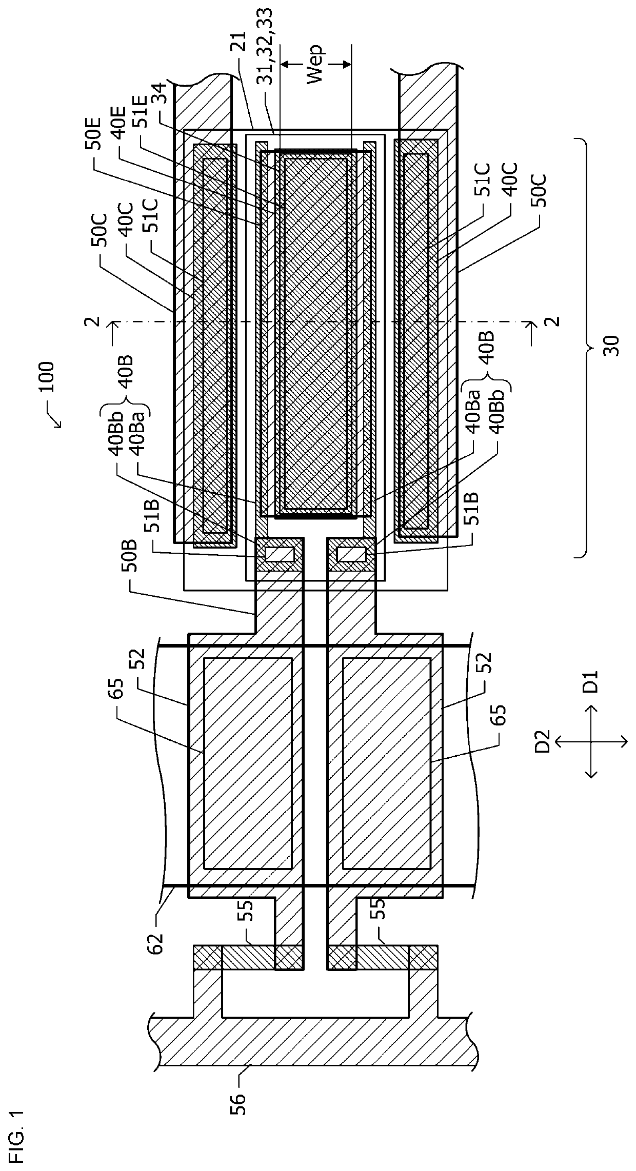
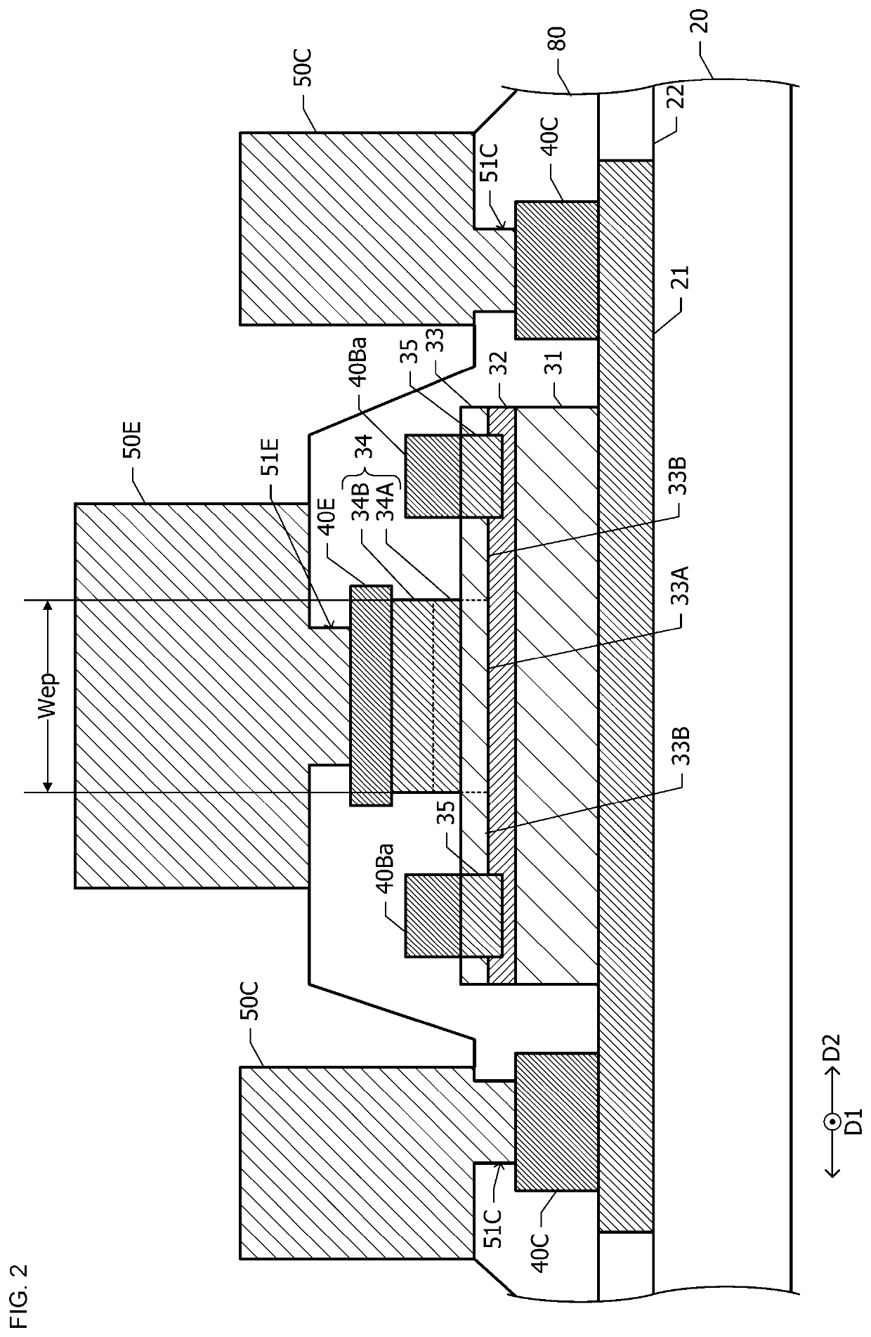
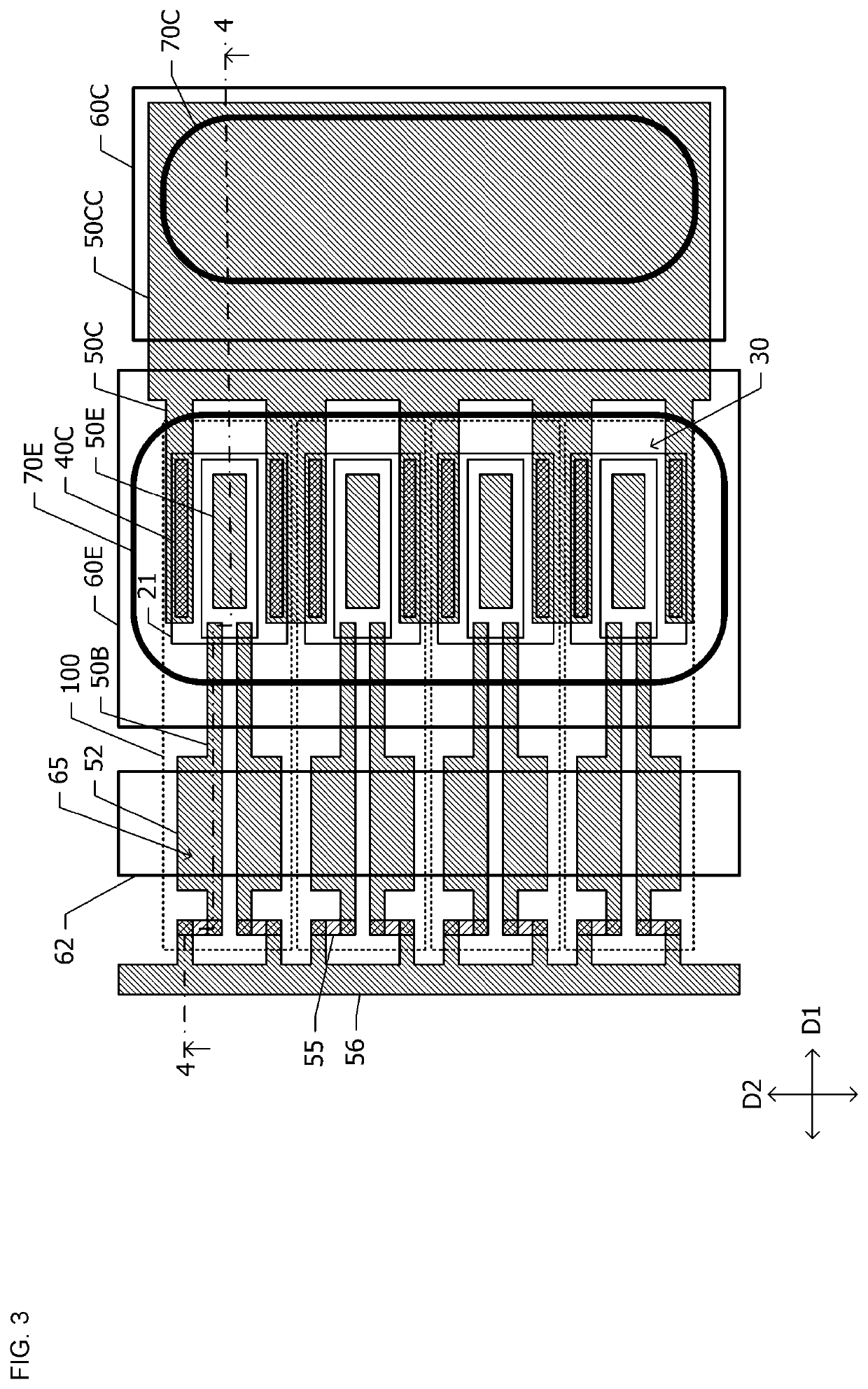
[0028]The following describes a unit cell in a first example and a power amplifier module including the unit cell, with reference to FIGS. 1 to 6.
[0029]FIG. 1 illustrates planar positional relationship between constituent elements of a unit cell 100 in the first example. The unit cell 100 includes a heterojunction bipolar transistor 30, two capacitors 65, and two resistance elements 55.
[0030]A substrate has a surface partially overlaid with a sub-collector layer 21, which has n-type conductivity. The sub-collector layer 21 is, for example, substantially rectangular when viewed in plan. A collector layer 31, a base layer 32, and an emitter layer 33 are located within the sub-collector layer 21 when viewed in plan. The collector layer 31 is a continuous region when viewed in plan. That is, the collector layer 31 viewed in plan is an integral whole instead of being divided into separate regions. The periphery of the base layer 32 and the periphery of the emitter layer 33 respectively c...
second example
[0097]The following describes the unit cell 100 in the second example with reference to FIGS. 8 and 9. Description of configurations identical to those of the unit cells 100 in the first example (see FIGS. 1 and 2) will be omitted.
[0098]FIG. 8 illustrates planar positional relationship between constituent elements of the unit cell 100 in the second example. FIG. 9 is a sectional view of the unit cell taken along dash-dot line 9-9 in FIG. 8. In the first example, the base layer 32 and the emitter layer 33 (see FIG. 1) are substantially rectangular when viewed in plan. The region between two base-electrode pad portions 40Bb viewed in plan is entirely overlaid with the base layer 32 and the emitter layer 33. A distinctive feature of the second example is that the region between two base-electrode pad portions 40Bb viewed in plan is overlaid with neither the base layer 32 nor the emitter layer 33. When viewed in plan, the base layer 32 and the emitter layer 33 each have a cutout portion...
third example
[0103]The following describes the unit cell 100 in the third example with reference to FIGS. 10 and 11. Description of configurations identical to those of the unit cell 100 in the first example (see FIGS. 1 and 2) will be omitted.
[0104]FIG. 10 illustrates planar positional relationship between constituent elements of the unit cell 100 in the third example. FIG. 11 is a sectional view of the unit cell taken along dash-dot line 11-11 in FIG. 10.
[0105]In the first example, the first-layer base lines 50B are connected to the corresponding base-electrode pad portions 40Bb. Distinctive features of the third example are that two base electrodes 40B do not include the base-electrode pad portions 40Bb and each have a substantially rectangular shape that is long in the first direction D1 when viewed in plan. Each base contact hole 51B is long in the longitudinal direction of the base electrodes 40B and extends from a point close to one end of the corresponding base electrode 40B to a point c...
PUM
 Abstract
Description
Claims
Application Information
 - R&D Engineer
- R&D Manager
- IP Professional
- Industry Leading Data Capabilities
- Powerful AI technology
- Patent DNA Extraction
Browse by: Latest US Patents, China's latest patents, Technical Efficacy Thesaurus, Application Domain, Technology Topic.
© 2024 PatSnap. All rights reserved.Legal|Privacy policy|Modern Slavery Act Transparency Statement|Sitemap