
Reinforcement learning pulse programming

Active Publication Date: 2021-04-08
SAMSUNG ELECTRONICS CO LTD
View PDF0 Cites 3 Cited by
  • Summary
  • Abstract
  • Description
  • Claims
  • Application Information

AI Technical Summary

Benefits of technology

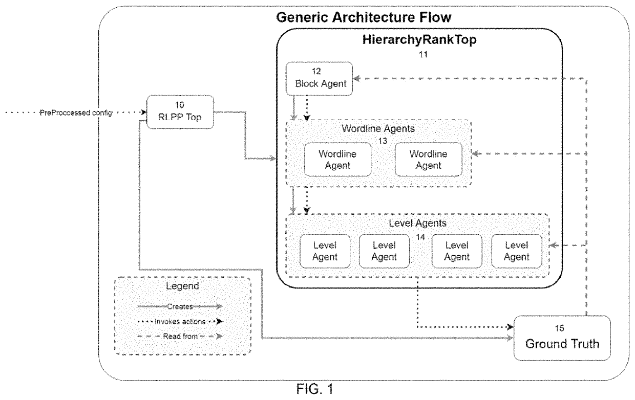
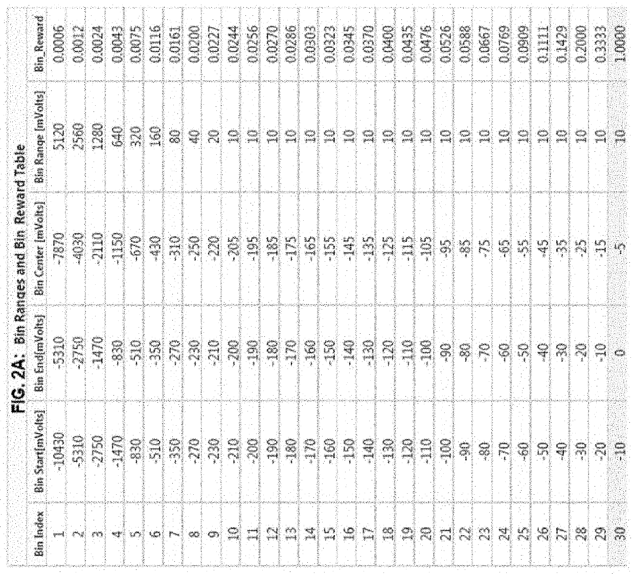
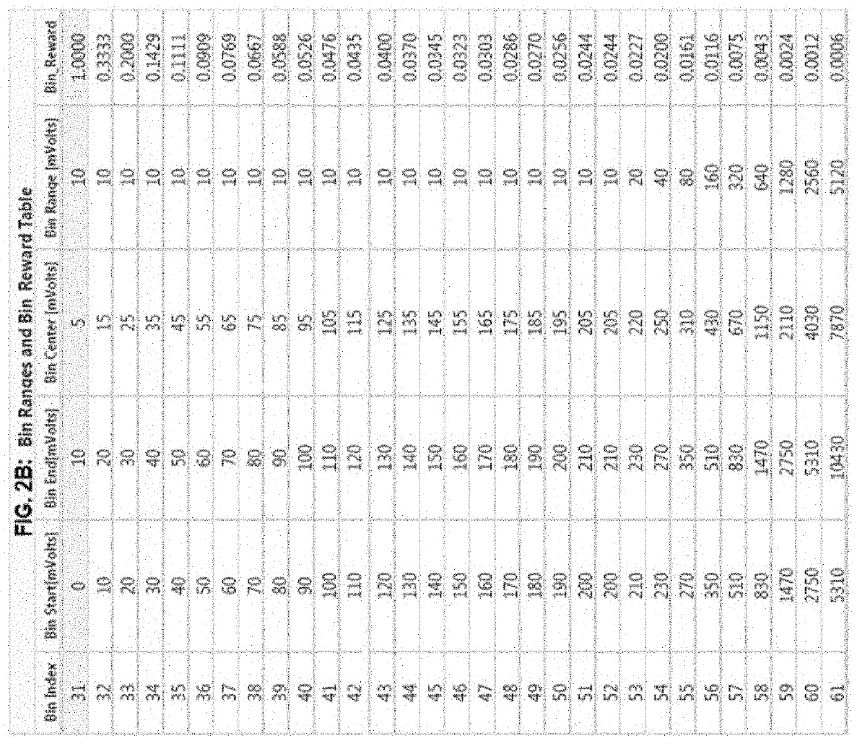
This patent is about a programming method for NAND flash memory using reinforcement learning. The method involves a software agent that learns to optimize its performance by interacting with the NAND flash environment. The interaction is done by applying programming actions to the NAND flash and receiving feedback in the form of observations related to the cell voltage states in the NAND flash and rewards related to the programming quality. The learning speed is increased by using advanced AI techniques such as hierarchical reinforcement learning (HRL) which breaks down the task to smaller subtasks and utilizes the hierarchical structure of the NAND flash. The method gives the optimal action in each state and can utilize function approximations to generalize across actions and states. The programming method results in high performance in an environment with inter cell programming disturbances and other NAND flash channel noise, and out-performs the established methods in both programming quality, low bit-error-rate (BER), and programming speed.

Problems solved by technology

However, storing more bits per cell decreases the dynamic voltage range of each voltage state making it more susceptible to noise.
As a result thereof, the reliability of flash memory decreases significantly and the performance of current programming algorithms is not sufficient.
During the process of programming a target voltage to a memory cell, the signal is subject to various distortions, noise conditions and other impairments.
Due to the above, programming a NAND flash is a noisy process: actions do not always go as planned and the writing outcome is not deterministic.
As a result, programming algorithm performance is severely degraded.
Since cell voltage levels at each cell cannot be precisely predicted after applying the programming pulse, there cannot be a plan for the entire sequence of pulses.

Method used


Image

  • Reinforcement learning pulse programming
  • Reinforcement learning pulse programming
  • Reinforcement learning pulse programming

Examples


Embodiment Construction

[0037]Exemplary embodiments of the disclosure as described herein generally provide systems and methods for training an agent to program different voltage levels to different cells. While embodiments are susceptible to various modifications and alternative forms, specific embodiments thereof are shown by way of example in the drawings and will herein be described in detail. It should be understood, however, that there is no intent to limit the disclosure to the particular forms disclosed, but on the contrary, the disclosure is to cover all modifications, equivalents, and alternatives falling within the spirit and scope of the disclosure.

[0038]NAND flash memories have a three-level hierarchy of block, wordline, and cell. The number of blocks varies between chip types but is usually in the order of several thousand per chip. A flash memory device can then consist of one or more such chips, so overall the amount of blocks per flash memory device varies quite a bit. The number of wordli...


PUM


Abstract

A NAND memory device that includes a plurality of blocks, each block comprises a plurality of wordlines and an associated agent, and each wordline comprises a plurality of cells and a plurality of voltage levels and an associated agent, and each voltage level comprises an agent. A method of programming the NAND memory device includes receiving, by an agent at a given rank in the plurality of ranks, parameters from a higher rank agent in the hierarchy of ranks and a state from the memory device; determining, by the agent, an action from the parameters and the state; passing the action as parameters to a lower rank agent in the hierarchy of ranks; and updating the agent based on a reward output by the agent, wherein the reward measures a difference between the target voltage levels of the cells and the actual voltage levels programmed to the cells.

Description

TECHNICAL FIELD[0001]Embodiments of the present disclosure are directed to an AI module that leans an optimal program method for a specific NAND memory device in terms of maximal capacity, minimal program noise, and maximal program speed.DISCUSSION OF THE RELATED ART[0002]To provide a combination of price and performance for a wide range of high-density storage applications, modern NAND flash memory chips enables storing several bits of data in each flash cell. This scheme is called a multi-level cell. A multi-level cell partitions the threshold voltage range of a flash cell into several voltage states and the written value is extracted from the cell voltage level. However, storing more bits per cell decreases the dynamic voltage range of each voltage state making it more susceptible to noise. As a result thereof, the reliability of flash memory decreases significantly and the performance of current programming algorithms is not sufficient.[0003]During the process of programming a t...

Claims


Application Information

Patent Timeline
IPC IPC(8): G06N3/08G06N3/04G11C16/04G11C16/10G11C16/08
CPCG06N3/08G06N3/04G11C16/08G11C16/10G11C16/0483G06N3/006G06N7/01G11C8/08G11C16/26
Inventor BLAICHMAN, EVGENYBERMAN, AMITHALPERIN, ELISHAELBAZ, DAN
Owner SAMSUNG ELECTRONICS CO LTD
Learn More