Method of topology-selective film formation of silicon oxide

a topology-selective film and silicon oxide technology, applied in the direction of coatings, metallic material coating processes, chemical vapor deposition coatings, etc., can solve the problems of difficult control of the topology of silicon oxide films, degradation of critical dimensions (cd) of trenches, and adverse effects on the underlying film, so as to improve the adsorption property of halogen-containing precursors, improve the surface conditions of substrates, and reduce the degree of adsorption of precursors

Active Publication Date: 2021-04-22
ASM IP HLDG BV
View PDF4 Cites 142 Cited by
  • Summary
  • Abstract
  • Description
  • Claims
  • Application Information

AI Technical Summary

Benefits of technology

[0025]In some embodiments, when the nitridation and the oxidization are conducted by PEALD, sometimes, the degree of adsorption of the precursor on the substrate surface becomes lowered upon the oxidization, and in that case, by improving the su

Problems solved by technology

However, when a thin film is subjected to etching, etching selectivity of the thin film, an underlying film, and a mask material, i.e., a degree of differences in resistance to etching among the thin film, the underlying film, and the mask material, is always an issue, and adverse effect on the underlying film (e.g., degradation of the quality of the underlying film by penetrated ion energy, and degradation of critical dimensions (CD) of a trench), for example, is inevitable.
However, controlling a topology of silicon oxide film is very difficult because oxidation occurs rather isotropically in a film deposition process.
In TS-SiN, the high wet-etching selectiv

Method used


Image

  • Method of topology-selective film formation of silicon oxide
  • Method of topology-selective film formation of silicon oxide
  • Method of topology-selective film formation of silicon oxide

Examples


example 1

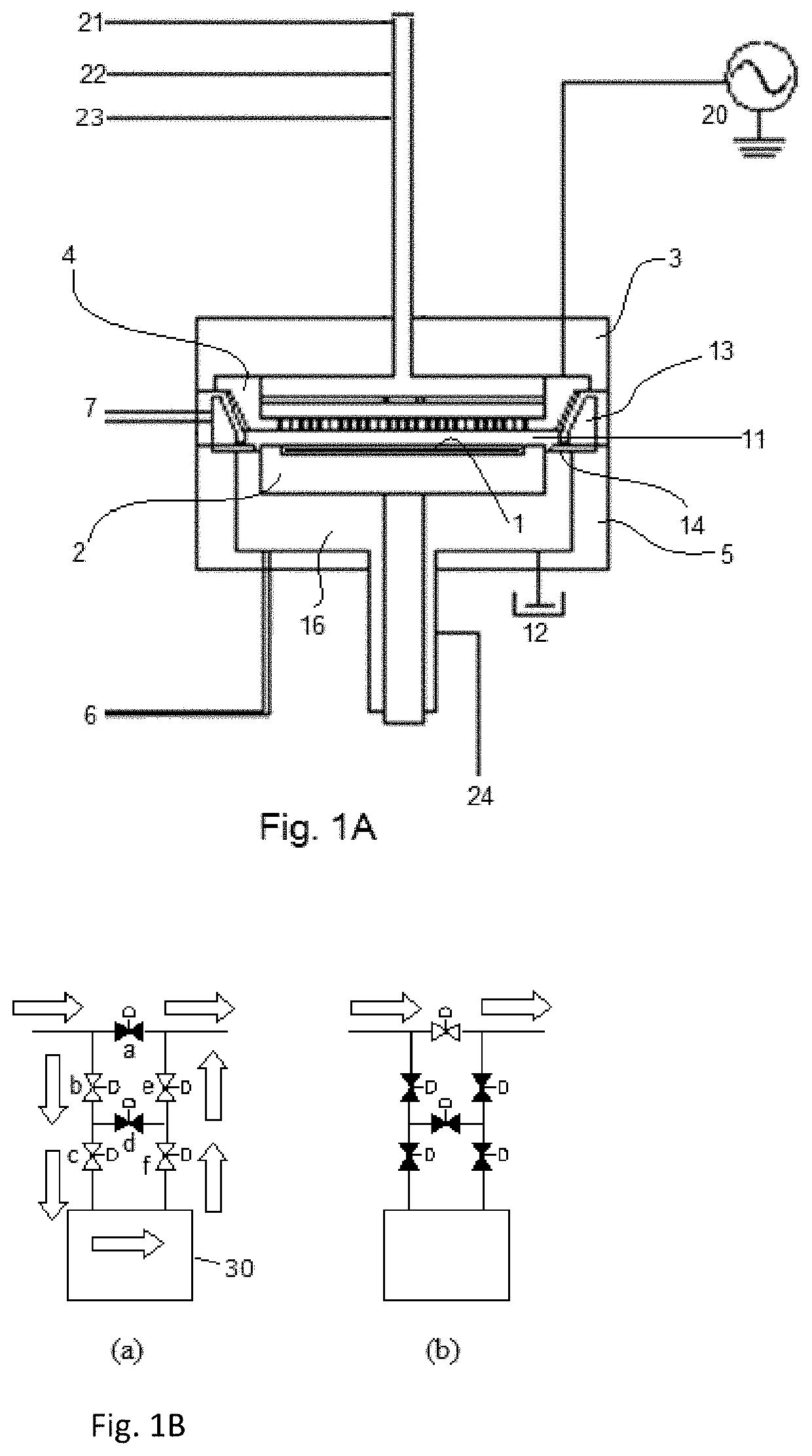
[0104]In this example, the selective reformation of a target portion of a film as illustrated in FIG. 5 was conducted. First, a SiN film having a thickness of 20 nm was formed on a Si substrate (0300 mm) having trenches (having an opening of 30 nm and an aspect ratio of 3) by PEALD, and then, the SiN film was converted to a SiO film according to the process sequence illustrated in FIG. 7 under the common conditions shown in Table 3 and the specific conditions shown in Table 4 below using the PEALD apparatus illustrated in FIG. 1A and a gas supply system (FPS) illustrated in FIG. 1B. Thereafter, the substrate was subjected to wet etching under the conditions shown in Table 3 below. As comparative examples, a SiO film was deposited in a manner similar to the above according to the process sequence illustrated in FIG. 8 wherein no nitridation / deposition process and no oxidation (conversion) process were conducted.

TABLE 3(numbers are approximate)Common Conditions for Nitridation / Deposit...


PUM

PropertyMeasurementUnit
Timeaaaaaaaaaa
Fractionaaaaaaaaaa
Fractionaaaaaaaaaa

Abstract

A method for forming a silicon oxide film on a step formed on a substrate includes: (a) designing a topology of a final silicon oxide film by preselecting a target portion of an initial silicon nitride film to be selectively deposited or removed or reformed with reference to a non-target portion of the initial silicon nitride film resulting in the final silicon oxide film; and (b) forming the initial silicon nitride film and the final silicon oxide film on the surfaces of the step according to the topology designed in process (a), wherein the initial silicon nitride film is deposited by ALD using a silicon-containing precursor containing halogen, and the initial silicon nitride film is converted to the final silicon oxide film by oxidizing the initial silicon nitride film without further depositing a film wherein a Si—N bond in the initial silicon nitride film is converted to a Si—O bond.

Description

CROSS-REFERENCE TO RELATED APPLICATIONS[0001]This application claims the benefit of U.S. Provisional Application No. 62 / 916,226, filed on Oct. 16, 2019, in the United States Patent and Trademark Office, the disclosure of which is incorporated herein in its entirety by reference.BACKGROUNDField of the Invention[0002]The present invention relates generally to a method for forming a silicon oxide film on a step having a top surface, a sidewall, and a bottom surface formed on a substrate, particularly, a method of topology-selective film formation of silicon oxide.Related Art[0003]Atomic layer deposition (ALD) methods including a plasma-enhanced atomic layer deposition (PEALD) method are widely used in semiconductor-manufacturing processes as a method of forming a conformal film on a substrate having a patterned surface. In some semiconductor-manufacturing processes, a film which has been formed once as a conformal film is subjected to dry etching or other dry trimming processes in orde...

Claims


Application Information

Patent Timeline
IPC IPC(8): H01L21/02H01L21/311C23C16/34C23C16/455C23C16/56
CPCH01L21/0223H01L21/0217H01L21/0228H01L21/02164H01L21/02252C23C16/56H01L21/02274H01L21/31111C23C16/345C23C16/45525H01L21/02249C23C16/45542C23C16/45534C23C16/402C23C16/04C23C16/045H01L21/02304H01L21/02326H01L21/31116H01L21/02211H01L21/02332H01L21/0234H01L21/02247H01L21/02271
Inventor FUKAZAWA, ATSUKIZAITSU, MASARUCHEN, PEI-CHIA
Owner ASM IP HLDG BV
Why Eureka
Try Eureka