Ultra-thin copper foil, ultra-thin copper foil with carrier, and method for manufacturing printed wiring board

Active Publication Date: 2021-04-29
MITSUI MINING & SMELTING CO LTD
View PDF0 Cites 0 Cited by
  • Summary
  • Abstract
  • Description
  • Claims
  • Application Information

AI Technical Summary

Benefits of technology

[0005]A packaging technique called two-and-a-half-dimensional (2.5D) implementation has been developed for achieving high-density packaging of semiconductor components and their high processing rates. In the 2.5D implementation, a silicon interposer as an intermediate substrate is provided between an integrated circuit (IC) chip and a package substrate. The silicon interposer intermediates the IC chip and the package substrate which have different terminal pitches. In other words, the silicon interposer serves as a rewiring substrate in the 2.5D implementation. In detail, an upper electrode and a lower electrode of the silicon interposer are electrically connected by a through-silicon via (TSV) formed in the silicon interposer. Highly dense trace

Problems solved by technology

Unfortunately, the silicon interposer and the glass interposer are expensive.
In addition, process costs, for example, for formation of a through-silicon via or a through-glass via (TGV) are also significantly high.
Thus, rewiring techniques using silicon interposers or glass interposers are employed in only limited fields, fo

Method used


Image

  • Ultra-thin copper foil, ultra-thin copper foil with carrier, and method for manufacturing printed wiring board
  • Ultra-thin copper foil, ultra-thin copper foil with carrier, and method for manufacturing printed wiring board
  • Ultra-thin copper foil, ultra-thin copper foil with carrier, and method for manufacturing printed wiring board

Examples


Example

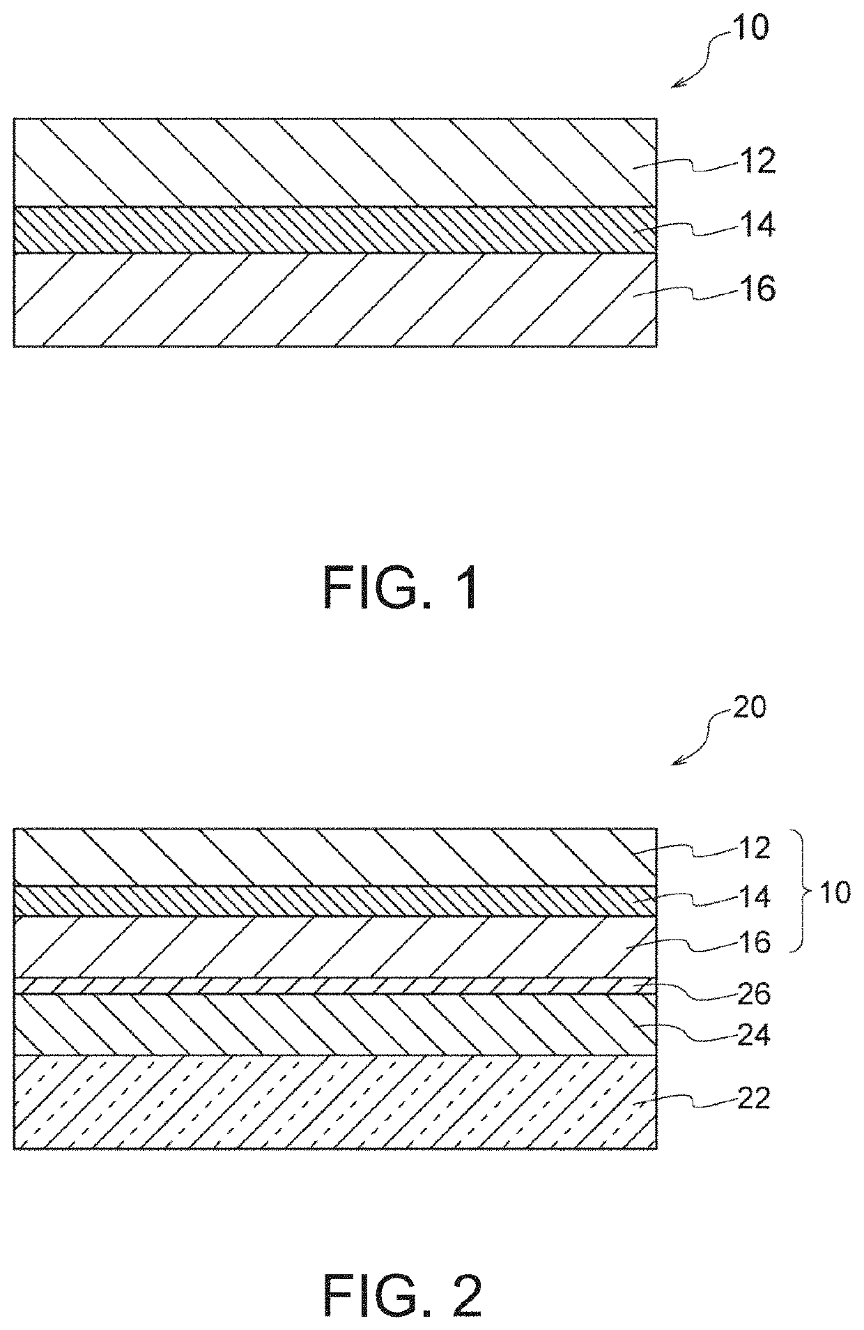
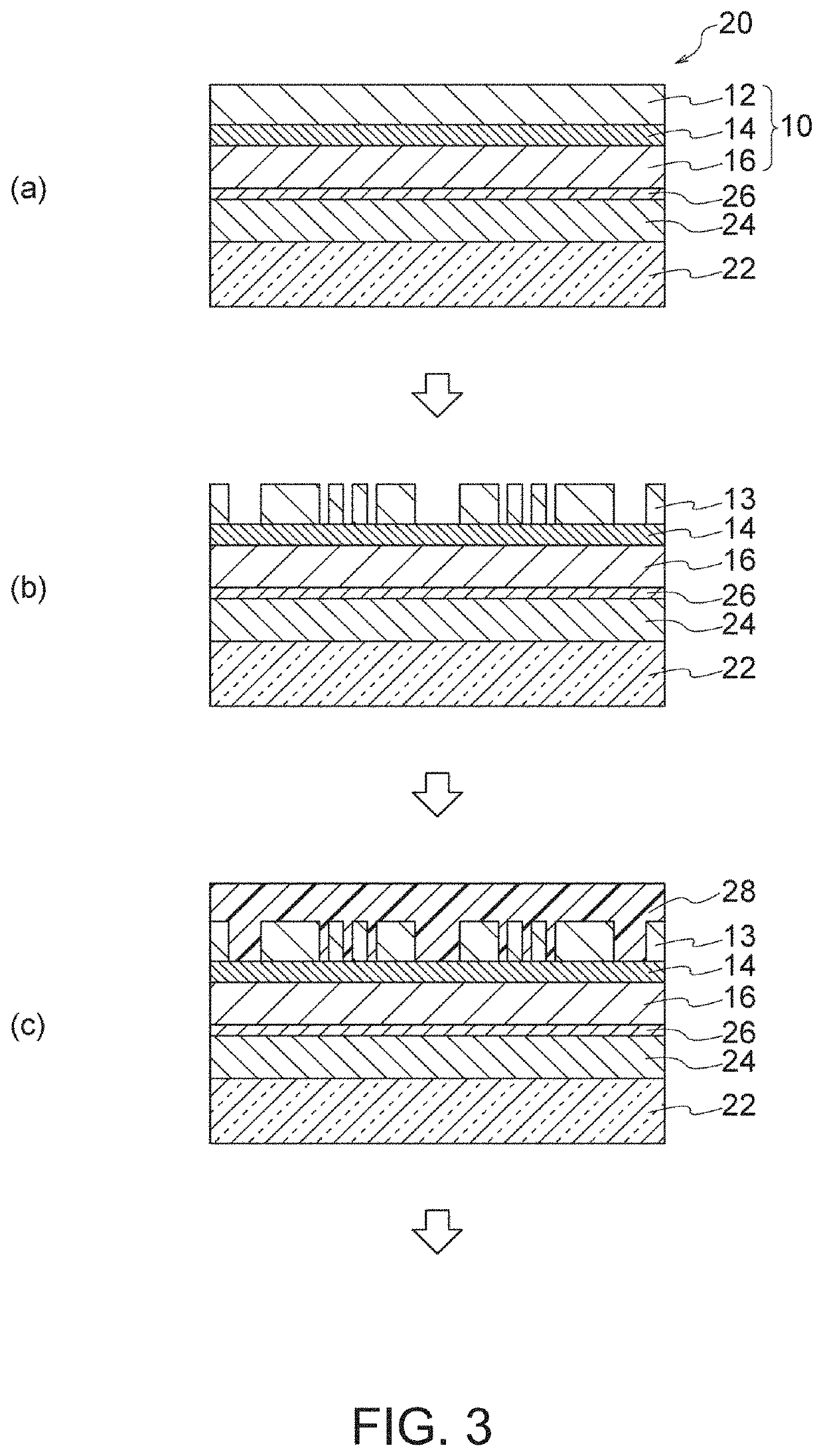
Extremely Thin Copper Foil

[0032]FIG. 1 schematically illustrates an extremely thin copper foil of the present invention. As illustrated in FIG. 1, an extremely thin copper foil 10 of the invention includes, in sequence, a first extremely thin copper layer 12, an etching stopper layer 14, and a second extremely thin copper layer 16. Two sides of the extremely thin copper foil 10 each have an arithmetic average roughness Ra of 20 nm or less. By forming a three-layer structure including the first extremely thin copper layer 12, the etching stopper layer 14, and the second extremely thin copper layer 16 in which two sides each have an arithmetic average roughness Ra of 20 nm or less, it is possible to provide the extremely thin copper foil 10 that enables formation of highly fine different wiring patterns with a line / space (L / S) of 10 μm or less / 10 μm or less on the two sides and is thus usable as an inexpensive and readily processable substitution for silicon and glass interposers. In ...


PUM

PropertyMeasurementUnit
Lengthaaaaaaaaaa
Fractionaaaaaaaaaa
Thicknessaaaaaaaaaa

Abstract

An extremely thin copper foil is provided that enables formation of highly fine different wiring patterns with a line/space (L/S) of 10 μm or less/10 μm or less on two sides of the copper foil and is thus usable as an inexpensive and readily processable substitution for silicon and glass interposers. The extremely thin copper foil includes, in sequence, a first extremely thin copper layer, an etching stopper layer, and the second extremely thin copper layer. Two sides of the extremely thin copper foil each have an arithmetic average roughness Ra of 20 nm or less.

Description

TECHNICAL FIELD[0001]The present invention relates to an extremely thin copper foil, an extremely thin copper foil with a carrier, and a method of manufacturing a printed circuit board.BACKGROUND ART[0002]Printed circuit boards with finer wiring patterns (finer pitches) have been required as electronic devices, such as mobile electronic devices, are compact and advanced. In order to meet such a request, preferred are copper foils for manufacture of printed circuit boards that have smaller thicknesses and lower surface roughnesses. For example, Patent Literature 1 (JP2005-76091A) discloses a method of manufacturing an extremely thin copper foil with a carrier, including laminating a release layer and an extremely thin copper foil in sequence on a smooth surface of a carrier copper foil, where the average surface roughness Rz of the carrier copper foil is reduced to 0.01 to 2.0 μm. Patent Literature 1 also discloses subjecting the extremely thin copper foil with a carrier to a process...

Claims


Application Information

Patent Timeline
IPC IPC(8): H05K3/46H05K1/09H05K3/06
CPCH05K3/4658H05K1/09H05K2203/0384H05K3/067H05K2203/0353H05K3/062B32B15/01H05K3/025H05K2203/016H05K3/20H05K1/186H05K2201/09118H05K2203/1572H05K2201/0317H05K2201/0361H05K3/108B32B15/018H01L23/49861H01L21/4828H01L23/49579H01L23/49548B32B15/20H01L23/12B32B2311/12B32B2307/538B32B2309/105
Inventor MATSUURA, YOSHINORI
Owner MITSUI MINING & SMELTING CO LTD
Why Eureka
Try Eureka