Image sensor employing avalanche diode and shared output circuit

Active Publication Date: 2021-06-17
PIXART IMAGING INC
View PDF0 Cites 0 Cited by
  • Summary
  • Abstract
  • Description
  • Claims
  • Application Information

AI Technical Summary

Benefits of technology

The present invention describes an image sensor that has a special kind of pixel called an SPAD. These pixels have several benefits. First, they allow for smaller pixels to be used, which means more pixels can be included in a camera without compromising image quality. Second, these pixels provide a high fill factor, which means they capture more light and produce better color representation. These benefits make it easier to create high-quality cameras with improved performance.

Problems solved by technology

However, the SPAD cannot accomplish the quenching by itself, and thus a quenching circuit is required in operation so as to quickly pull down a bias voltage of the SPAD to be lower than a breakdown voltage after an avalanche occurs.

Method used


Image

  • Image sensor employing avalanche diode and shared output circuit
  • Image sensor employing avalanche diode and shared output circuit
  • Image sensor employing avalanche diode and shared output circuit

Examples


first embodiment

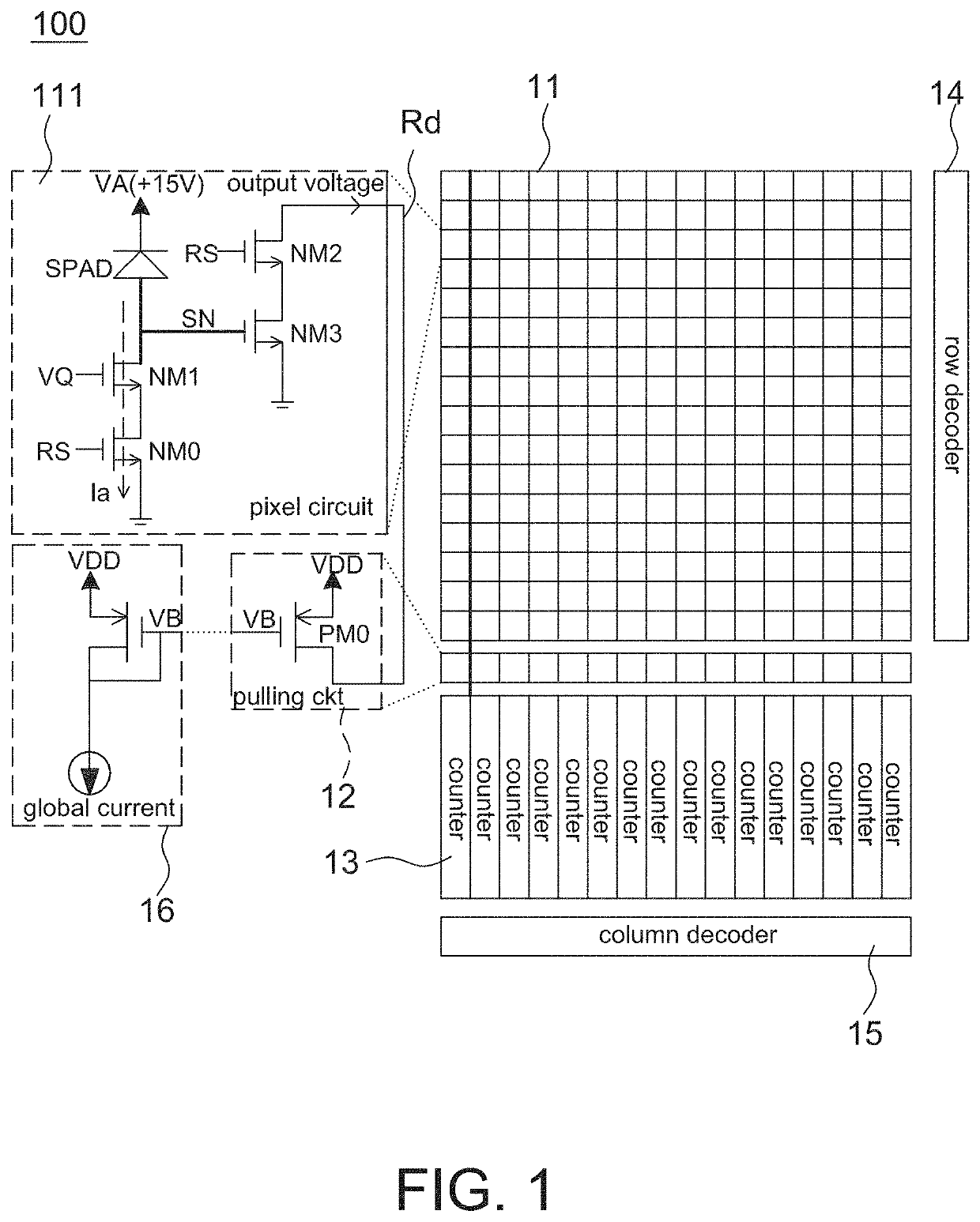
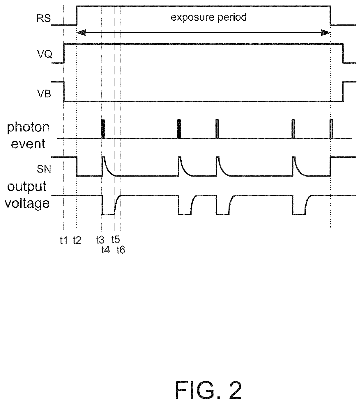
[0031]Referring to FIG. 1, it is a schematic diagram of an image sensor 100 according to the present disclosure. The image sensor 100 is used to detect extremely weak light and high frequency signals, and thus a single photon avalanche diode (SPAD) is employed to detect photon events. A processor generates an image frame by counting photon events of every pixel to perform the object tracking, gesture recognition, 3D image construction, and biological feature detection and recognition.

[0032]The image sensor 100 includes a pixel array 11, a plurality of pulling circuits 12, a plurality of counters 13, a row decoder 14, a column decoder 15 and a global current source circuit 16, wherein the row decoder 14 and the column decoder 15 are used to determine a pixel position in the pixel array 11 that is being exposed and outputting a detected signal (e.g., pulses mentioned below). The operation of the row decoder 14 and the column decoder 15 is known to the art and is not a main objective o...

second embodiment

[0050]Referring to FIG. 4, it is a schematic diagram of an image sensor 400 according to the present disclosure. The image sensor 400 is also used to detect extremely weak light and high frequency signals, and thus a single photon avalanche diode (SPAD) is employed to detect photon events. A processor generates an image frame by counting photon events of every pixel to perform the object tracking, gesture recognition, 3D image construction, and biological feature detection and recognition.

[0051]The image sensor 400 includes a pixel array 41, a plurality of pulling circuits 42, a plurality of counters 43, a row decoder 44, a column decoder 45 and a global current source circuit 46, wherein the row decoder 44 and the column decoder 45 are also used to determine a pixel position in the pixel array 41 that is being exposed and outputting a detected signal (e.g., pulses mentioned below).

[0052]The pixel array 41 includes a plurality of pixel circuits 411 (e.g., FIG. 4 also showing 16×16 p...

third embodiment

[0070]In the third embodiment, the image sensor 100 also includes a pixel array 11, a plurality of pulling circuits 12, a plurality of counters 13, a row decoder 14, a column decoder 15 and a global current source circuit 16. The pixel array 11 also includes a plurality of pixel circuits 111.

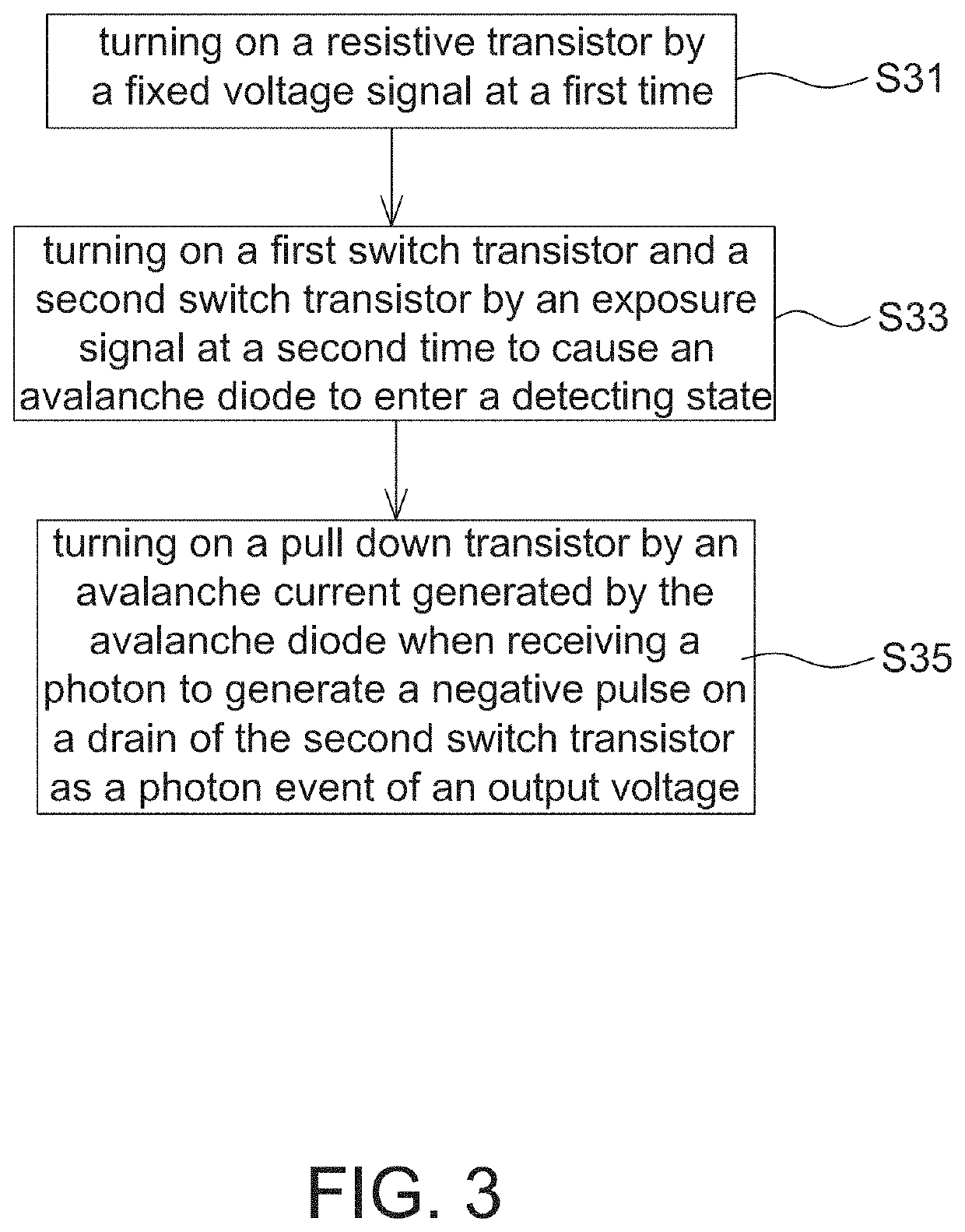
[0071]Each pixel circuit 111 includes an avalanche diode SPAD and at least a transistor NM3. A cathode of SPAD is connected to a positive bias voltage VA, e.g., +15V, but not limited to. An anode of SPAD is connected to a node SN that connects to a gate of the transistor NM3. Each of the plurality of pulling circuits 12 is configured to be coupled to a drain of the transistor NM3 of each pixel circuit 111 of one pixel circuit column via a readout line Rd.

[0072]Furthermore, to control the pixel circuit 111 in one pixel circuit column to detect a photo event sequentially, each pixel circuit 111 further includes another transistor NM2 connected between the transistor NM3 and the readout line Rd. Op...


PUM


Abstract

There is provided an image sensor employing an avalanche diode. The image sensor includes a plurality of pixel circuits arranged in a matrix, a plurality of pulling circuits, a plurality of output circuits and a global current source circuit. Each of the plurality of pixel circuits includes a single photon avalanche diode and a P-type or N-type select switch transistor. Each of the plurality of pulling circuits is arranged corresponding to one pixel circuit column. The global current source circuit is used to form a current mirror with each of the plurality of pulling circuits. Each of the plurality of output circuits is shared by at least two pixel circuits.

Description

CROSS REFERENCE TO RELATED APPLICATION[0001]The present application is a continuation-in-part application of U.S. Ser. No. 16 / 872,626, filed on May 12, 2020, which is a divisional application of U.S. Ser. No. 16 / 258,673, filed on Jan. 28, 2019, the disclosures of which are hereby incorporated by reference herein in their entirety.BACKGROUND1. Field of the Disclosure[0002]This disclosure generally relates to the photon detection technology and, more particularly, to an image sensor employing a single photon avalanche diode (SPAD) in the pixel circuit. The quenching and readout circuit of the SPAD has a low limitation on minimum pixel unit and a high fill factor.2. Description of the Related Art[0003]Single photon detection is a good choice in dealing with weak light environment and high frequency light signals.[0004]For example, a single photon avalanche diode (SPAD) can be used as a detector for weak light, and has the benefits of high avalanche gain, fast response and low power con...

Claims


Application Information

Patent Timeline
IPC IPC(8): H04N5/378H04N5/374H01L27/146
CPCH04N5/378H04N5/374H01L31/107H01L27/14643H01L27/14612H04N25/77H04N25/778H04N25/78H04N25/75H04N25/76
Inventor HUANG, SEN-HUANGTSAI, TSO-SHENG
Owner PIXART IMAGING INC
Why Eureka
Try Eureka