Method of producing cell culture chip

a cell culture chip and cell technology, applied in the direction of manufacturing tools, photomechanical equipment, instruments, etc., can solve the problem of easy liquid leakage from the flow path, and achieve the effect of stable production of a fine flow path structur

Active Publication Date: 2021-07-22
TOKYO OHKA KOGYO CO LTD
View PDF0 Cites 0 Cited by
  • Summary
  • Abstract
  • Description
  • Claims
  • Application Information

AI Technical Summary

Benefits of technology

[0013]According to the present invention, it is possible to provide a method of producing a cell culture chip, which enables stable production of a fine flow path structure and in which liquid leakage from the flow path is suppressed.

Problems solved by technology

However, in the cell culture chip produced by the production method described in Japanese Unexamined Patent Application, First Publication No. 2018-102236, there is a problem in that liquid leakage from the flow path may easily occur while a culture solution at approximately 37° C. is allowed to flow in a case where the chip has a complicated flow path structure.

Method used


Image

  • Method of producing cell culture chip
  • Method of producing cell culture chip
  • Method of producing cell culture chip

Examples


first embodiment

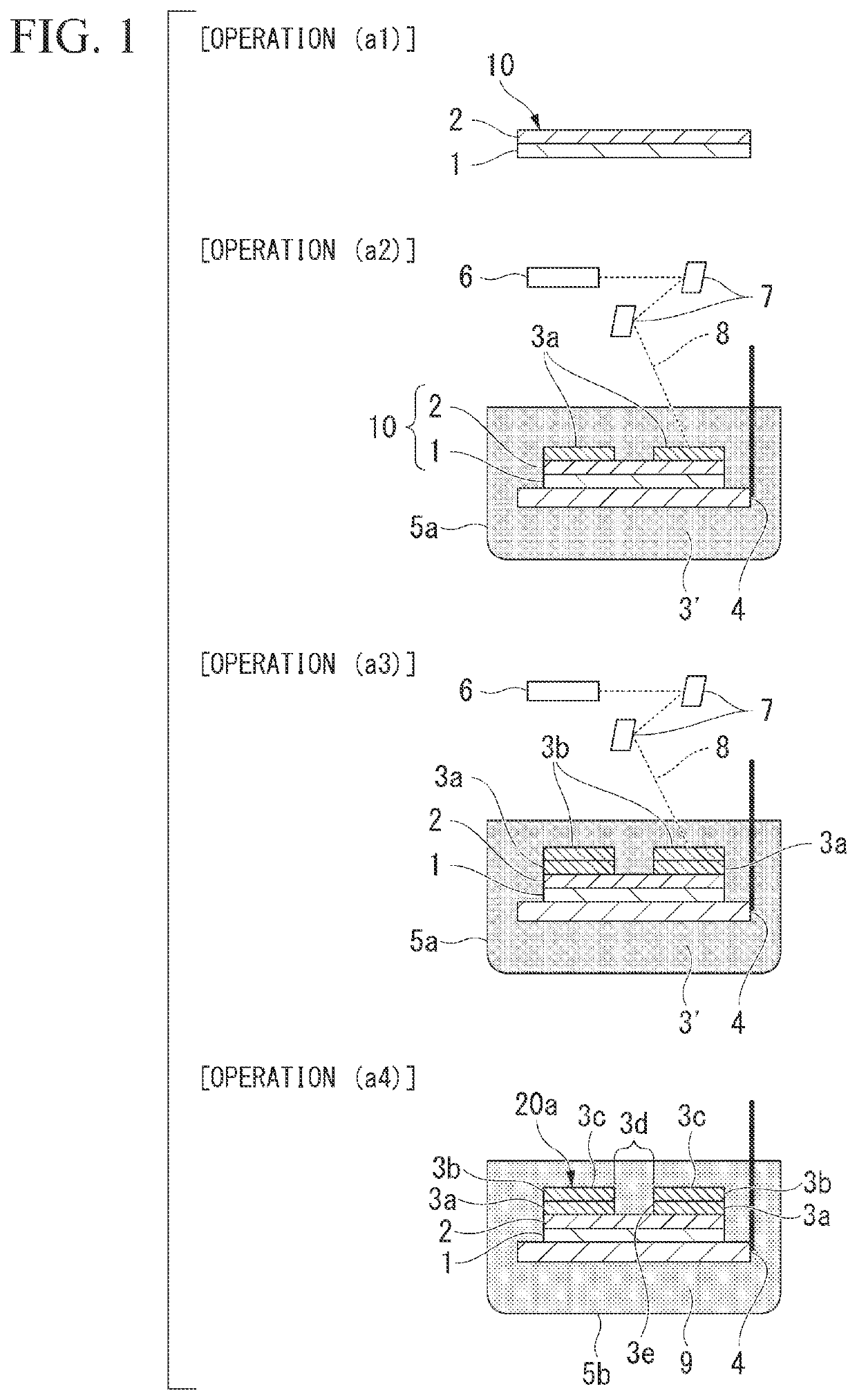
[0027]As the method of producing a cell culture chip, a method in which a 3D printer is applied to a shaping method may be exemplified. Hereinafter, as the method of producing a cell culture chip according to the embodiment, a production method including the above-described steps A, B, and C, in which the above-described step A includes the following operations (a1) to (a4) will be described.

[0028]The operation (a1) is an operation of forming a photosensitive adhesive layer by coating the substrate having transparency with a photosensitive adhesive to obtain a 3D printing substrate.

[0029]The operation (a2) is an operation of selectively irradiating a photosensitive shaping material layer obtained by film-forming a photosensitive shaping material on the 3D printing substrate with ultraviolet rays to selectively cure the photosensitive shaping material layer.

[0030]The operation (a3) is an operation of further film-forming a photosensitive shaping material, allowing a photosensitive sh...

examples

[0188]Hereinafter, the present invention will be described in more detail with reference to examples, but the present invention is not limited to these examples.

[Production Example 1] Production of Cell Culture Chip

[0189]As a microflow path chip for a cell assay, a cell culture chip including a microflow path structure (X) having a hollow structure illustrated in FIG. 7 was produced in the following manner.

[0190]1. Preparation of Cell Culture Flow Path Substrate: Step A

[0191](1-1) Preparation of First Photosensitive Adhesive

[0192]The raw materials listed in Table 1 below were sufficiently stirred to obtain a uniform solution, thereby obtaining a first photosensitive adhesive.

TABLE 1Name of raw materialParts by massARONIX M313 (manufactured by Toagosei Co., Ltd.)100IRGACURE 184 (manufactured by BASF SE)3Propylene glycol monomethyl ether acetate (PGMEA)100

[0193](1-2) Preparation of 3D Printing Substrate

[0194]Next, a surface (an easy-adhesion treated surface) of a lubricative layer 102...


PUM

PropertyMeasurementUnit
glass transition temperatureaaaaaaaaaa
thicknessaaaaaaaaaa
thicknessaaaaaaaaaa

Abstract

A method of producing a cell culture chip, in which a first adhesive is film-formed on a first substrate having transparency such that a first adhesive layer and a recessed portion on which one or more cell culture flow paths are formed face each other, and a second adhesive is film-formed on the first substrate such that a second adhesive layer and a flat portion around the recessed portion face each other, thereby obtaining a cell culture flow path substrate, the first adhesive containing a polyester-based resin having a glass transition temperature of 5° C. or higher, and the second adhesive containing a polyester-based resin having a glass transition temperature of lower than 5° C.

Description

BACKGROUND OF THE INVENTIONField of the Invention[0001]The present invention relates to a method of producing a cell culture chip.[0002]Priority is claimed on Japanese Patent Application No. 2020-008704, filed on Jan. 22, 2020, the content of which is incorporated herein by reference.Description of Related Art[0003]A frequently occurring problem of monolayer culture which has been used for cell assays of the related art is that the environment surrounding cells is greatly different from that in a living body, and many of the functions exhibited in the body are lost in the cultured cells. It is expected that the above-described problem is solved by recent advances in microfabrication technology and 3D culture technology so that the throughput and reliability of cell assays are improved at the same time. In particular, the concept of organ-on-a-chip, which handles cell culture chips provided with a microfluidic device that reproduces a physiological three-dimensional culture environme...

Claims


Application Information

Patent Timeline
Patent Type & Authority Applications(United States)
IPC IPC(8): C12M3/06B32B37/12
CPCC12M23/16B32B2310/0831B32B2037/1253B32B37/12C12M33/00B33Y10/00G03F7/0037B29C64/124B33Y80/00G03F7/027G03F7/2051
Inventor FUJIMOTO, TAKASHIMAENO, EMIFUJII, YASUSHIKUMAZAWA, HIROTSUGU
Owner TOKYO OHKA KOGYO CO LTD
Why Eureka
Try Eureka