High capacity memory circuit with low effective latency

a memory circuit and low effective latency technology, applied in the field of memory circuits and computing systems, can solve the problems of difficult formation of thin-film memory arrays over the cua, dense low-voltage logic circuit sense amplifiers are particularly susceptible to degradation, etc., to achieve fast access times, high data density, and high endurance

Active Publication Date: 2021-08-12
SUNRISE MEMORY CORP
View PDF3 Cites 7 Cited by
  • Summary
  • Abstract
  • Description
  • Claims
  • Application Information

AI Technical Summary

Benefits of technology

[0015]The integrated circuit of the present invention make possible many new applications because of high data density, high endurance and high-speed access achievable by the quasi-volatile memory circuit on the memory chip, while the faster memory circuits on the companion chip provide even faster access times, the combination resulting effectively in a high-density, low-latency memory circuit, essentially a heterogeneous memory with advantages that can be exploited in new applications. For example, the integrated circuit of the present invention is particularly suitable for in-memory computing or near-memory computing applications.

Problems solved by technology

Forming thin-film memory arrays over the CuA poses challenges.
The dense low-voltage logic circuit are particularly susceptible to degradation resulting from exposure to the thermal cycles.
For example, sense amplifiers are particularly susceptible to degradation under thermal processing, which adversely impacts their sensitivity and signal integrity.
The large number of manufacturing steps required to form both the CuA and the memory circuits adversely affects the potential yield and performance.
The medium-voltage or high-voltage circuitry are generally not as scalable as the low-voltage circuitry, making them less cost-effective when manufactured under advanced manufacturing process nodes.
Such a process compromises the scaling and the performance in the low-voltage transistors that would otherwise be possible.
Thus, by placing both high-voltage, medium-voltage, and low-voltage circuits on the second substrate, Lu's peripheral circuits can only be manufactured on the second substrate using a manufacturing process that is capable of forming all of the low-voltage logic circuits and the medium-voltage and high-voltage analog circuitry, thus compromising both the high-voltage and low-voltage transistors.
Such faster memory circuits may be volatile or non-volatile memory circuits.

Method used


Image

  • High capacity memory circuit with low effective latency
  • High capacity memory circuit with low effective latency
  • High capacity memory circuit with low effective latency

Examples


Embodiment Construction

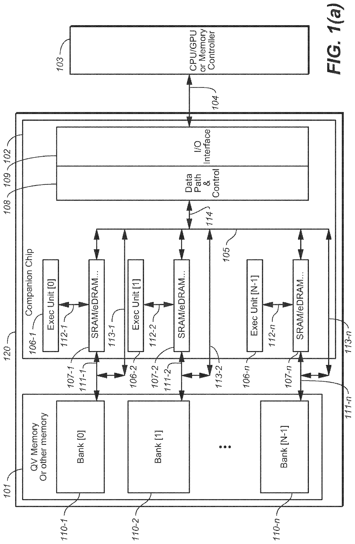
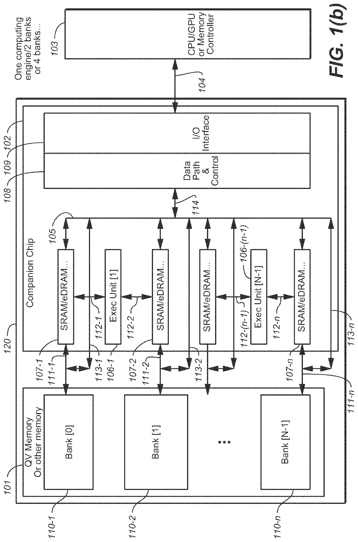
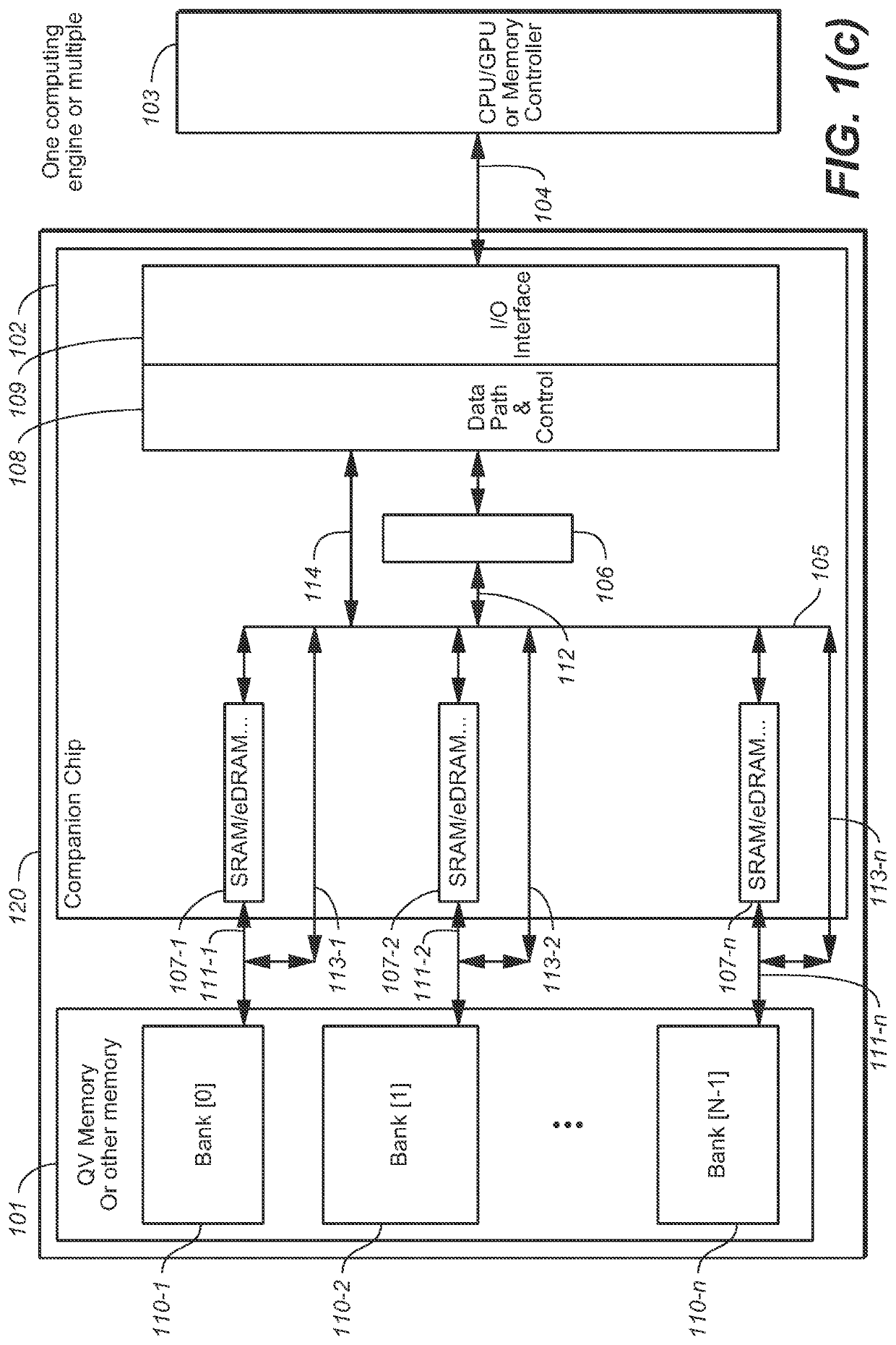
[0042]According to one embodiment of the present invention, an integrated circuit may be formed by combining high-density, quasi-volatile memory circuits, or non-volatile memory circuits, formed on a first semiconductor die (“memory chip”), and faster memory circuits (e.g., SRAM, DRAM, eDRAM, MRAM, eMRAM, PCM or any other suitable memory circuits) formed on a second semiconductor die (“companion die”). The quasi-volatile memory circuits or the non-volatile memory circuits on the memory chip are preferably built for high density, such as achieved through three-dimensional construction. In contrast, the faster memory circuits on the companion chip are preferably built for high performance, such as achieved through more advanced logic process nodes. The memory chip and the companion chip may be brought together by high-density hybrid bonding, for example.

[0043]Of importance, in one embodiment of the present invention, both the memory chip and the companion chip are organized in modular...


PUM


Abstract

A first circuit formed on a first semiconductor substrate is wafer-bonded to a second circuit formed on a second memory circuit, wherein the first circuit includes quasi-volatile or non-volatile memory circuits and wherein the second memory circuit includes fast memory circuits that have lower read latencies than the quasi-volatile or non-volatile memory circuits, as well as logic circuits. The volatile and non-volatile memory circuits may include static random-access memory (SRAM) circuits, dynamic random-access memory (DRAM) circuits, embedded DRAM (eDRAM) circuits, magnetic random-access memory (MRAM) circuits, embedded MRAM (eMRAM), or any suitable combination of these circuits.

Description

CROSS REFERENCE TO RELATED APPLICATION[0001]The present application is related to and claims priority of U.S. provisional patent application (“Parent Provisional Application”, Ser. No. 62 / 971,720, entitled “High Capacity Memory Circuit With Low Effective Latency,” filed on Feb. 7, 2020.[0002]The present application is also related to (i) U.S. non-provisional application (“Non-provisional Application I”), Ser. No. 16 / 776,279, entitled “Device with Embedded High-Bandwidth, High-Capacity Memory using Wafer Bonding,” filed on Jan. 29, 2020, and (ii) U.S patent application (“Non-provisional Application II”), Ser. No. 16 / 582,996, entitled “Memory Circuit, System and Method for Rapid Retrieval of Data Sets,” filed on Sep. 25, 2019; (III) U.S. non-provisional patent application (“Non-provisional Application III”), Ser. No. 16 / 593,642, entitled “Three-dimensional Vertical NOR Flash Thin-film Transistor Strings,” filed on Oct. 4, 2019; (iv) U.S. non-provisional patent application (“Non-provis...

Claims


Application Information

Patent Timeline
Patent Type & Authority Applications(United States)
IPC IPC(8): G06F3/06H01L23/00H01L25/18
CPCG06F3/0611H01L24/20G06F3/0631H01L2224/214H01L2924/1435H01L2924/1431H01L2224/211H01L25/18G11C7/1048G11C7/1006H01L2224/08145H01L24/80H01L24/08
Inventor KIM, YOUN CHEULCHERNICOFF, RICHARD S.QUADER, KHANDKER NAZRULNORMAN, ROBERT D.YAN, TIANHONGSALAHUDDIN, SAYEEFHARARI, ELI
Owner SUNRISE MEMORY CORP
Why Eureka
Try Eureka