BiSb Topological Insulator with Novel Buffer Layer that Promotes a BiSb (012) Orientation

a topological insulator and buffer layer technology, applied in the field of buffer layer, can solve the problem of poor adhesion of the bisb layer with a (012) orientation on si (111)

Active Publication Date: 2021-08-12
TOKYO INST OF TECH +1
View PDF7 Cites 10 Cited by
  • Summary
  • Abstract
  • Description
  • Claims
  • Application Information

AI Technical Summary

Problems solved by technology

However, adhesion of the BiSb layer wi...

Method used


Image

  • BiSb Topological Insulator with Novel Buffer Layer that Promotes a BiSb (012) Orientation
  • BiSb Topological Insulator with Novel Buffer Layer that Promotes a BiSb (012) Orientation
  • BiSb Topological Insulator with Novel Buffer Layer that Promotes a BiSb (012) Orientation

Examples


examples

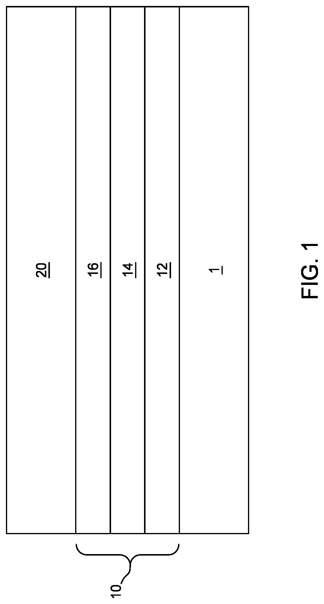
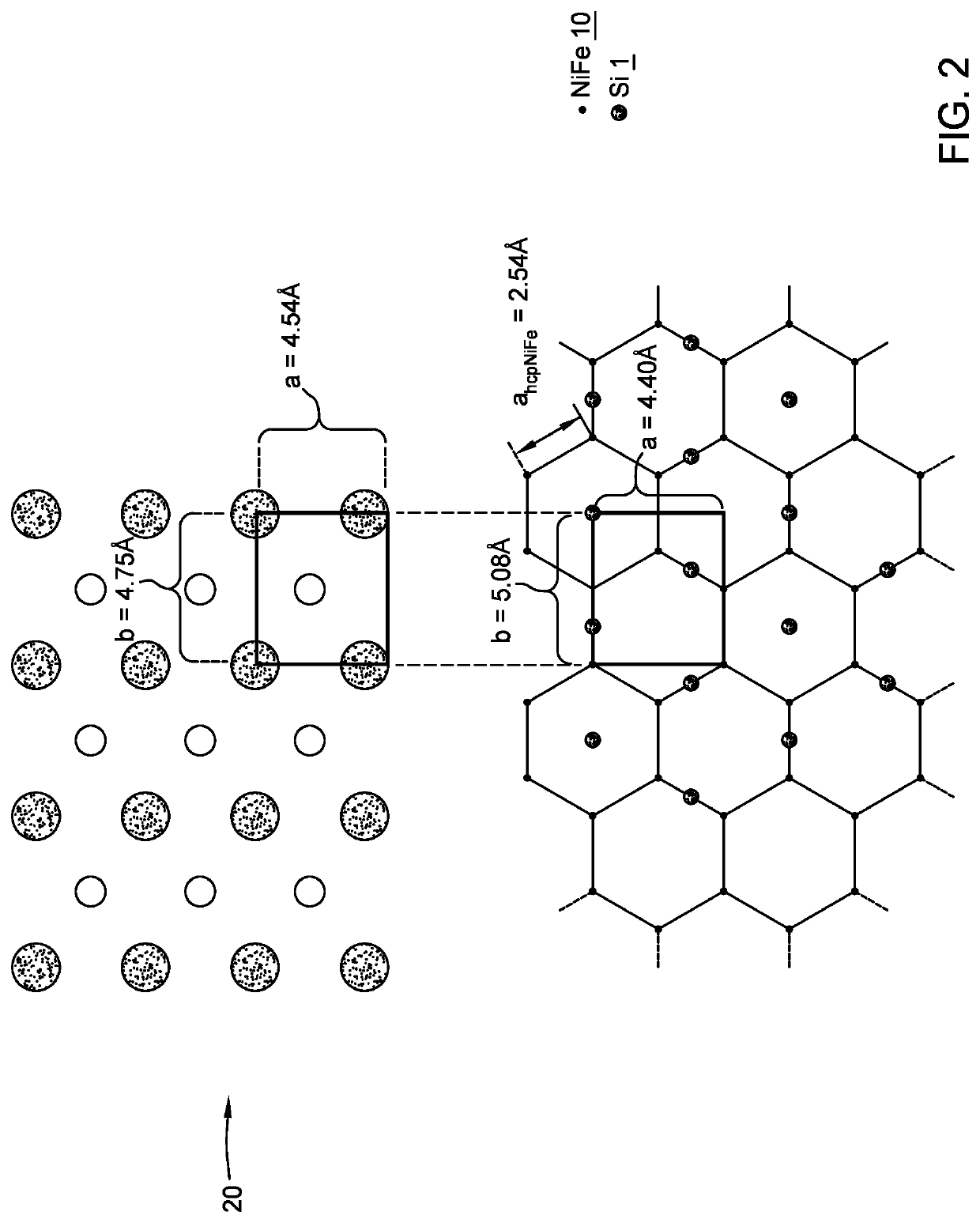
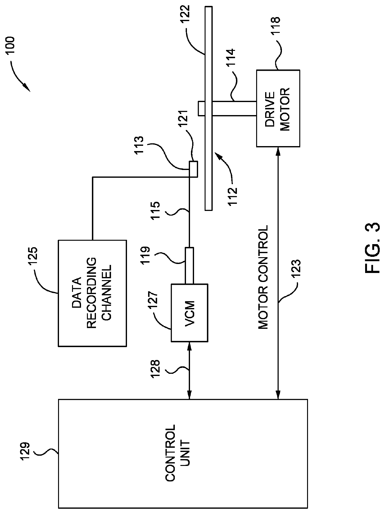
[0062]The following are examples to illustrate various embodiments of a BiSb layer, such as the BiSb layer 20 of FIGS. 1 and 2, the magnetic drive 100 of FIG. 3, the write head 210 of FIG. 4, the SOT devices 250 of FIGS. 5A-C and 6, other BiSb layers, other magnetic drives, other SOT devices, and variations thereof. These examples are not meant to limit the scope of the claims unless specifically recited in the claims.

example a

[0063]In Example A (FIG. 7), a BiSb layer 710 was deposited by PVD to a thickness of about 100 Å directly on a silicon (111) substrate. A BiSb layer 720 was deposited by PVD to a thickness of about 100 Å directly on a NiFe layer. The NiFe layer was deposited by PVD to a thickness of about 6 Å over a silicon (111) substrate. A BiSb layer 730 was deposited by PVD to a thickness of about 100 Å directly on a NiFe layer. The NiFe layer was deposited by PVD to a thickness of about 50 Å over a silicon (111) substrate.

[0064]FIG. 7 illustrates X-ray diffraction (XRD) 2Θ scans of the BiSb layers 710, 720, 730. The BiSb layer 710 directly formed on a thermal oxide coated silicon substrate showed a (001) orientation. The BiSb layers 720, 730 directly formed on NiFe layers over a thermal oxide coated silicon substrates showed a (012) orientation.

example b

[0065]In Example B (FIG. 8), a BiSb layer 1010 was deposited by PVD to a thickness of about 100 Å directly on a Cu layer. The Cu layer was deposited by PVD to a thickness of about 20 Å over a thermal oxide coated silicon substrate. A BiSb layer 1020 was deposited by PVD to a thickness of about 100 Å directly on a NiFe layer. The NiFe layer was deposited by PVD to a thickness of about 10 Å over a thermal oxide coated silicon substrate. A BiSb layer 1030 was deposited by PVD to a thickness of about 100 Å directly on a NiTa layer. The NiTa layer was deposited by PVD to a thickness of about 20 Å over a thermal oxide coated silicon substrate. A BiSb layer 1040 was deposited by PVD to a thickness of about 100 Å directly on a NiFe layer. The NiFe layer was deposited to a thickness of about 5 Å by PVD directly on a Cu layer. The Cu layer was deposited by PVD to a thickness of about 20 Å over a thermal oxide coated silicon substrate. A BiSb layer 1050 was deposited by PVD to a thickness of a...


PUM


Abstract

A spin-orbit torque (SOT) magnetic tunnel junction (MTJ) device includes a substrate, a buffer layer formed over the substrate, and a bismuth antimony (BiSb) layer formed over the buffer layer, the BiSb layer having a (012) orientation. In certain embodiments, the SOT MTJ device is part of a microwave assisted magnetic recording (MAMR) write head. In certain embodiments, the SOT MTJ device is part of a magnetoresistive random access memory (MRAM) device.

Description

CROSS-REFERENCE TO RELATED APPLICATIONS[0001]This application claims benefit of U.S. provisional patent application Ser. No. 62 / 975,661, filed Feb. 12, 2020, which is herein incorporated by reference.BACKGROUND OF THE DISCLOSUREField of the Disclosure[0002]Embodiments of the present disclosure generally relate to a buffer layer that promotes growth of a bismuth antimony (BiSb) layer having a (012) orientation.Description of the Related Art[0003]BiSb is a material that has been proposed as a spin Hall layer for spin torque oscillator (STO) and magnetoresistive random access memory (MRAM) devices. BiSb is a narrow gap topological insulator with both giant spin Hall effect and high electrical conductivity.[0004]N. H. D. Khang, Y. Ueda, and P. N. Hai, “A conductive topological insulator with large spin Hall effect for ultralow power spin-orbit torque switching,” Nature Materials, v. 17, 808 (2018), discovered that BiSb with a (012) crystallographic orientation has a high spin Hall angle...

Claims


Application Information

Patent Timeline
IPC IPC(8): G11B5/11H01L27/22H01L43/04H01L43/06H01L43/10H01F10/32G11B5/147
CPCG11B5/11H01L27/222H01L43/04H01L43/06G11B2005/0024H01F10/3254H01F10/3272H01F10/329G11B5/147H01L43/10H10N50/80H10N50/10H10N50/85H10B61/00H10N52/00H10N52/80
Inventor LE, QUANGHWANG, CHERNGYEYORK, BRIAN R.NGUYEN, THAO A.GAO, ZHENGHO, KUOK SANHAI, PHAM NAM
Owner TOKYO INST OF TECH
Why Eureka
Try Eureka