Fin-type field effect transistor and formation method thereof

A fin-type field effect and transistor technology, which is applied in semiconductor devices, semiconductor/solid-state device manufacturing, electrical components, etc., can solve the problem that the carrier mobility cannot be satisfied.

Active Publication Date: 2015-03-18
SEMICON MFG INT (SHANGHAI) CORP
View PDF3 Cites 8 Cited by
  • Summary
  • Abstract
  • Description
  • Claims
  • Application Information

AI Technical Summary

Problems solved by technology

[0006] The problem solved by the invention is that with the expansion of information data in modern society, faster and more eff...

Method used

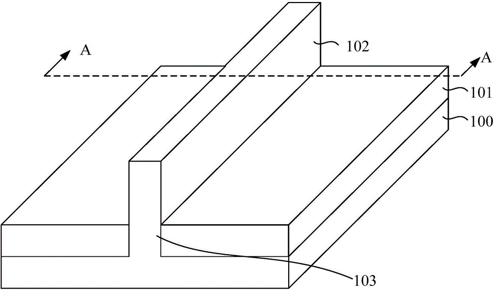
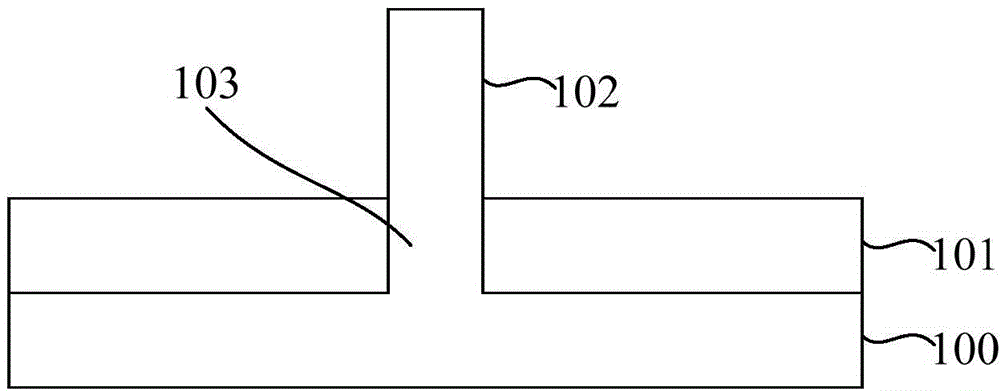

Image

  • Fin-type field effect transistor and formation method thereof
  • Fin-type field effect transistor and formation method thereof
  • Fin-type field effect transistor and formation method thereof

Examples


Embodiment Construction

[0060] Aiming at the problem of the background technology, the present invention proposes a scheme of applying the existing topological insulator material to the fin field effect transistor.

[0061] Topological insulator (Topological Insulator, TI) is a new state of matter with strange quantum properties, and it is one of the important scientific hotspots and frontiers of physics in recent years. It is completely different from "metal" and "insulator" in the traditional sense. It is a metallic state in which the interior is insulating and the interface allows charge movement. In other words, the bulk electronic state of a topological insulator is an insulator with a gap, while its surface is a gapless metallic state. However, this gapless surface metal state is completely different from the surface state caused by surface unsaturated bonds or surface reconstruction in the general sense, that is, unlike metals in the traditional sense, the surface metal state of topological in...


PUM


Abstract

Disclosed are a fin-type field effect transistor and a formation method thereof. The formation method of the fin-type field effect transistor includes the following steps: providing a substrate and forming a fin part on the substrate; selectively growing a topological insulator layer on the surface of the fin part; forming a gate dielectric layer which covers the topological insulator layer and forming a first gate electrode which crosses the insulating dielectric layer; respectively removing the gate dielectric layer and the topological insulator layer at the two ends of the fin part and forming epitaxial layers with doping on the surface of the exposed fin part, wherein the epitaxial layers are separated with the first gate electrode by the remaining gate dielectric layer and the topological insulator layer, and the epitaxial layers with doping, at the two ends of the fin part, are used as a source electrode and a drain electrode respectively; applying a voltage between the source electrode and the drain electrode so that the surface of the topological insulator layer is switched on and the surface of the topological insulator layer is used as a channel area; and applying a voltage between the gate electrode and the source electrode, wherein an electric field caused by the voltage is capable of adjusting the carrier concentration on the surface of the topological insulator body. Carriers in the channel area do not collide or interfere so that the mobility ratio of the carriers is improved.

Description

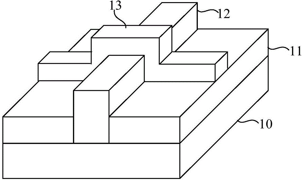
technical field [0001] The invention relates to the technical field of semiconductors, in particular to a fin field effect transistor and a forming method thereof. Background technique [0002] In the field of semiconductor technology, with the continuous reduction of the feature size of integrated circuits and the requirement for higher signal transmission speed of integrated circuits, transistors need to have higher driving current while gradually reducing their size. To meet this requirement, the length of conventional complementary metal oxide semiconductor (CMOS) transistors has become shorter than before, however, it is still difficult to meet the requirements of high integration. [0003] Therefore, in the prior art, a Fin Field Effect Transistor (FinFET) has been proposed. refer to figure 1 The fin field effect transistor comprises: an insulating layer 11 located on a substrate 10; a fin 12 penetrating through the insulating layer 11 and higher than the upper surfa...

Claims


Application Information

Patent Timeline
IPC IPC(8): H01L21/336H01L21/28H01L29/78H01L29/423
CPCH01L29/1037H01L29/26H01L29/66795H01L29/785
Inventor 张海洋王冬江
Owner SEMICON MFG INT (SHANGHAI) CORP
Why Eureka
Try Eureka